Previous: Introduction and Background Up: Introduction and Background Next: Basics and Terminology
General-purpose computers have served us well over the past couple of decades. Broad applicability has led to wide spread use and volume commoditization. Flexibility allows a single machine to perform a multitude of functions and be deployed into applications unconceived at the time the device was designed or manufactured. The flexibility inherent in general-purpose machines was a key component of the computer revolution.
To date, processors have been the driving engine behind general-purpose computing. Originally dictated by the premium for active real estate, processors focus on the heavy reuse of a single or small number of functional units. With Very Large Scale Integration (VLSI), we can now integrate complete and powerful processors onto a single integrated circuit, and the technology continues to provide a growing amount of real estate.
As enabling as processors have been, our appetite and need for computing power has grown faster. Despite the fact that processor performance steadily increases, we often find it necessary to prop up these general-purpose devices with specialized processing assists, generally in the form of specialized co-processors or ASICs. Consequently, today's computers exhibit an increasing disparity between the general-purpose core and its specialized assistants. High performance systems are built from a plethora of specialized ASICs. Even today's high-end workstations dedicate more active silicon to specialized processing than to general-purpose compute. The general-purpose processor will be only a small part of tomorrow's multi-media PC. As this trend continues, the term ``general-purpose computer'' will become a misnomer for modern computer systems. Relatively little of the computing power in tomorrow's computers can be efficiently deployed to solve any problem.
The problem is not with the notion of general-purpose computing, but with the implementation technique. For the past several years, industry and academia have focussed largely on the task of building the highest performance processor, instead of trying to build the highest performance general-purpose computing engine. When active area was extremely limited, this was a very sensible approach. However, as silicon real estate continues to increase far beyond the space required to implement a competent processor, it is time to re-evaluate general-purpose architectures in light of shifting resource availability and cost.
In particular, an interesting space has opened between the extremes of general-purpose processors and specialized ASICs. That space is the domain of reconfigurable computing and offers all the benefits of general-purpose computing with greater performance density than traditional processors. This space is most easily seen by looking at the binding time for device function. ASICs bind function to active silicon at fabrication time making the silicon useful only for the designated function. Processors bind functions to active silicon only for the duration of a single cycle, a restrictive model which limits the amount the processor can accomplish in a single cycle while requiring considerable on-chip resources to hold and distribute instructions. Reconfigurable devices allow functions to be bound at a range of intervals within the final system depending on the needs of the application. This flexibility in binding time allows reconfigurable devices to make better use of the limited device resources including instruction distribution.
Consequently, reconfigurable computing architectures offer:
The thesis provides:
The major contributions of this thesis include:
The remainder of this chapter provides a synopsis of the key
results and relationships developed in the thesis. This introductory part
of the thesis continues with Chapter which defines the
terminology and metrics used throughout the thesis.
Chapter
reviews and highlights the existing evidence for
the high performance potential of reconfigurable computing architectures.
Part sets the stage by examining the
computational capabilities of existing general-purpose computing devices.
This starts with a broad, empirical, review of general-purpose
architectures in Chapter
. In Chapter
, we
compare hardwired and general-purpose multiplier implementations as a case
study bridging general-purpose and application-dedicated architectures.
In Chapter
, we review processor architectures
implemented on top of reconfigurable architectures to broaden the picture
and to see one way in which conventional reconfigurable architectures deal
with high operational diversity.
Part takes a more compositional view of
reconfigurable computing architectures. Chapter
looks at
building blocks, sizes, and requirements for interconnect.
Chapter
looks at resource requirements for instruction
distribution. Finally in Chapter
, we bring the empirical data,
interconnect, and instruction characteristics together, providing a first
order model of RP-space, our high-level model for reconfigurable
processing architectures.
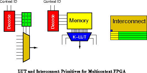
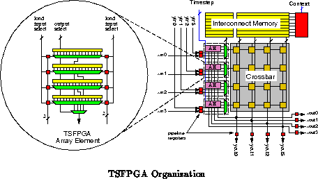
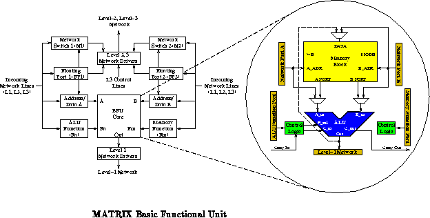
Part includes three new architectures: DPGA
(Chapters
and
), TSFPGA (Chapter
), and
MATRIX (Chapter
), which are highlighted below in
Section
. The final chapters in Part
,
review the results and identify promising directions for the future.
Broadly considered, reconfigurable devices fill their silicon area with a large number of computing primitives, interconnected via a configurable network. The operation of each primitive can be programmed as well as the interconnect pattern. Computational tasks can be implemented spatially on the device with intermediates flowing directly from the producing function to the receiving function. Since we can put thousands of reconfigurable units on a single die, significant data flow may occur without crossing chip boundaries. To first order, one can think about turning an entire task into hardware dataflow and mapping it on the reconfigurable substrate. Reconfigurable computing generally provides spatially-oriented processing rather than the temporally-oriented processing typical of programmable architectures such as microprocessors.
The key differences between reconfigurable machines and conventional processors are:
To establish an intuitive feel for the design point and role of configurable devices, we can take a high-level look at conventional devices. Ignoring, for the moment multiplies, floating-point operations, and table lookup computations, the modern processor has a peak performance on the order of 256, 3-LUT gate-evaluations per clock cycle ( e.g. two 64-bit ALUs). A modern FPGA has a peak performance on the order of 2,048, 4-LUT gate-evaluations per clock cycle. The basic clock cycle time is comparable giving the FPGA at least an order of magnitude larger raw capacity.
Note that both the processor ALUs and FPGA blocks are typically built with additional gates which serve to lower the latency of word operations without increasing the raw throughput ( e.g. fast carry chains which allow a full 64-bit wide add to complete within one cycle time). This latency reduction may be important to reducing the serial path length in tasks with limited parallelism, but is not reflected in this raw capacity comparison.
The FPGA can sustain its peak performance level as long as the same 2K gate-evaluation functionality is desired from cycle to cycle. Wiring and pipelining limitations are the primary reason the FPGA would achieve lower than peak performance, and this is likely to account for, at most, a 20-50% reduction from peak performance. If more diverse functionality is desired from a single FPGA than the 1-2K gate-evaluations provided by the FPGA, performance drops considerably due to function reload time.
The processor is likely to provide a much lower peak performance and the effect is much more application specific. Due to the bitwise-SIMD nature of traditional ALUs, work per cycle can be as low as a couple of gate-evaluations on compute operations. Since processors perform all ``interconnect'' using shifts, moves, loads, and stores, many cycles yield no gate-evaluations, only movement of data. The lower peak performance of processors comes from the fact that the processor ALU occupies only a small fraction of the die, with substantial area going to instruction flow control and on-chip memory to support large sequences of diverse operations without requiring off-chip instruction or data access.
A comparably sized, dedicated piece of hardwired functionality,
with no memory could provide a capacity of 200,000-300,000 4-LUT
gate-evaluations per clock cycle, at potentially higher clock rates. While
the raw gate delay on the hardwired logic can be 10 smaller than on
the FPGA, reasonable cycle times in equivalent logic processes are closer
to 2
since it makes sense to pipelined the FPGA design at a more
shallow logic depth than the custom logic. Returning to the multiplier,
for example, such a chip might provide 64K multiply bit operations per
cycle ( e.g. a 256
256 multiply pipelined at the byte level).
The dedicated hardware provides 100-300 times the capacity of the FPGA on
the one task it was designed to solve. To first order, the dedicated
hardware can deliver very little capacity to significantly different
applications. It is also worthwhile to note that the fixed granularity of
hardwired devices often causes them to sacrifice much of their capacity
advantage when used on small data items. For instance, performing an
8
8 multiply on a 64
64 hardwired multiplier makes use of
only
'th of the multiplier's capacity, removing much of its
300
capacity advantage.
Combining these observations, we can categorize the circumstances under which the various structures are prefered.
In Chapter we define our evaluation and comparison metrics
more carefully. Chapters
and
provide an
empirical review of conventional general-purpose and specialized
architectures, focusing on their performance density.
While reconfigurable devices have, potentially, 100 less
performance per unit area than hardwired circuitry, they provide
10-100
the performance density of processors. As noted above,
FPGAs offer a potential 10
advantage in raw, peak, general-purpose
functional density over processors. This density advantage comes largely
from dedicating significantly less instruction memory and distribution
resources per active computing element. At the same time this lower memory
ratio allows reconfigurable devices to deploy active capacity at a finer
grained level, allowing them to realize a higher yield of their raw
capacity, sometimes as much as 10
, than conventional processors.
It is these two effects taken together which give reconfigurable
architectures their 10-100
performance density advantage over
conventional processor architectures in many situations.
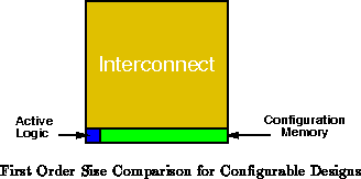
From an empirical review of conventional, reconfigurable devices, we see
that 80-90% of the area is dedicated to the switches and wires making up
the reconfigurable interconnect. Most of the remaining area goes into
configuration memory for the network. The actually logic function only
accounts for a few percent of the area in a reconfigurable device.
This interconnect and configuration overhead is responsible
for the 100 density disadvantage which
reconfigurable devices suffer relative to hardwired logic.
To a first order approximation, this gives us:
It is this basic relationship (Shown diagrammatically in
Figure ) which characterizes the RP
design space.
After reviewing implementations in Chapter ,
Chapters
and
examine
interconnect and instruction delivery issues in depth. Chapter
brings these together, yielding a slightly more sophisticated model than
the one above to explain the primary tradeoffs in the design of
reconfigurable computing architectures.
From the general relationships above, we see that conventional conventional Field Programmable Gate Arrays (FPGAs) represent one extreme in our RP-space. The space is large, leaving considerable space for interesting architectures in middle. Exploiting the relative area properties identified above and common device usage scenarios, we have developed three new general-purpose computing architectures. By judicious allocation of device resources, these architectures offer higher yielded capacity over a wide range of applications.
Ultimately, reconfiguration is a technique for compressing the resources dedicated to instruction stream distribution while maintaining a general-purpose architecture. As such, it is an important architectural tool for extracting the highest performance from our silicon real estate. Characteristics of an application which change slowly or do not change can be configured rather than broadcast. The savings in instruction control resources result in higher logic capacity per unit area.
With CMOS VLSI we have reached to the point where we are no longer so limited by the aggregate capacity of a single IC die that the device must be optimized exclusively to maximize the number of distinct instructions resident on a chip. Beyond this point spatial implementation of all or portions of general-purpose computations is both feasible and beneficial. From this point on we will see:
The thesis closes in Part by reviewing the key lessons
from reconfigurable designs and their implications for future
general-purpose architectures.