Previous: Empirical Review Up: Empirical Review Next: Case Study: Multiply
Here we review various general-purpose computing architectures by taking an empirical look at their implementations during the past decade. In this section we draw from the whole realm of general-purpose architectures -- not just those which fit directly into our RP-space. This makes a larger set of design points avilable for review, but also introduces considerably more variation in architectures than we will focus on in later chapters. We look primarily at general-purpose capacity in this section, generally ignoring the effects of specialized functional units. The following chapter will look at the effects of custom multipiers, the most common specialized functional unit added to nominally general-purpose computing devices. The focus here is on integrated, single IC, computational building blocks to keep the comparison as consistent as possible across such a wide variety of architectures. Additionally, we focus entirely on MOS VLSI implementations since most of these architecture have had multiple MOS VLSI implementations and the effects of MOS feature size device scaling are moderately well understood.
We start by looking at a simple RISC-style processor.
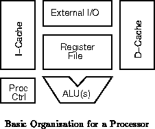
The pedagogical processor model (Figure ) is
composed of:
multicols
We extract a maximum of gate evaluations (
ALU bit
operations) per cycle. Modern processors are achieving cycle times as low
as 2-5ns with
. The fastest, single-ALU processors today thus offer
a peak capacity around 84 gate-evaluations/ns.
Table
compares several processor implementations
over the past decade. Results are summarized there in terms of ALU bit ops
since that is the native, and hence most accurate, unit for processors.
From Table
, we see that conventional processors
have provided a peak functional density of 3-9 ALU bit
operations/
over the past decade. We see from
Table
and some simple weightings below that an ALU bit op is
somewhere between one half and two 3-LUT gate evaluations.
It is interesting, and perhaps a bit unexpected, to note how consistent this capacity density has been over time. We might have expected:
This peak computational density assumes that every operation on each
-bit ALU performs an
-bit compute operation and the processor
completes one instructions per ALU on every cycle. In practice, a
significant number of processor cycles are not spent executing compute
operations.
For example, while HaL's SPARC64 should be able to issue 4
instructions per cycle, in practice it only issues 1.2 instructions per
cycle on common workloads [EG95]. Thus
%, resulting in
a 70% reduction from expected peak capacity.
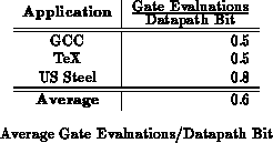
Assuming the integer DLX instructions mixes given in Appendix C of
[HP90] are typical, we can calculate
by weighting the
instructions by their provided capacities from Table
.
In Table
we see that one ALU bit op in these applications
is roughly 0.6 gate-evaluations.
If this effect is jointly typical with the instructions per issue
slot number above, then we would yield at most
of the theoretical, functional density. For the HaL case, this reduces
to
.
There are, of course, several additional aspects which prevent most any application from achieving even this expected peak capacity and which cause many applications to not even come close to it.
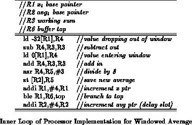
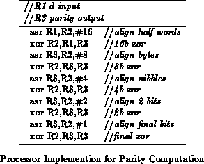
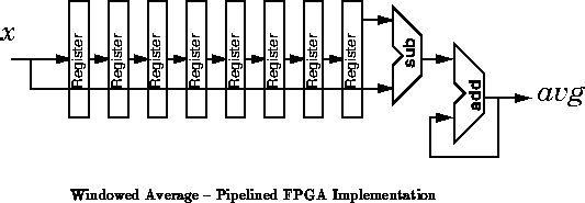
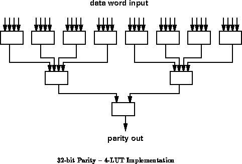
In 10 operations (See Figure ), the processor can perform
the 32b XOR required for the parity calculation -- 32 2-input gate
evaluations or 11 4-input gate evaluations. Again, assuming a MIPS-X like
processor and 1 CPI, we yield:
Very Long Instruction Word (VLIW) machines are processors with multiple, parallel functional units which are exposed at the architectural level. A single, wide, instruction word controls the function of each functional unit on a cycle-by-cycle basis. Pedagogically, a VLIW processor looks like a processor with multiple, independent functional units. At this level, the VLIW processor does not look characteristically different from the modern superscalar processors included at the end of the processor table.
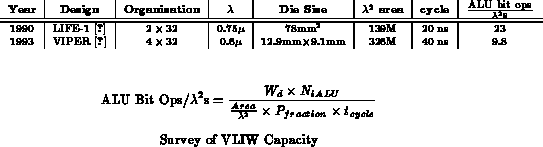
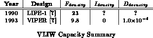
Table summarizes the characteristics of two
VLIW processors. With only two datapoints it is not possible to assess
general trends. These examples seem to have about 2
the peak
capacity of processors. To the extent this may be characteristic of VLIW
designs, it may arise from the fact that the separate functional units
share instruction control and management circuitry more than in superscalar
processors.
VLIW processors may fail to achieve their peak for the same reasons as processors. In addition, they may suffer from:
Digital Signal Processors (DSPs) are essentially specialized microprocessors which:
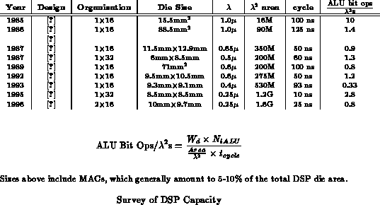
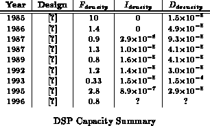
Table reviews several DSP implementations. On
non-multiply operations, the peak performance is generally lower than the
processors. For the kinds of operations typical of DSPs, these processors
will generally yield much closer to their peak capacity than processors.
Most general-purpose devices use memories to store instructions and data. A memory can also be used directly to implement complex computational functions. For complicated functions, a memory lookup can often provide high, programmable computational capacity. For just a few examples see [Lev77][RS92][HT95][Has87].
We characterize a memory by:
We can use a counting argument to determine how
complicated the functions can get. We start by observing that an -input,
one-output lookup table can implement
different functions. We
then consider how many gates it requires to implement any of these
functions. Each gate can be any function of four inputs, so each gate can
implement
functions. A collection of
gates can thus
implement at most
functions (less due to
overcounting). In order to implement any of the
functions provided by the table, we need at least:
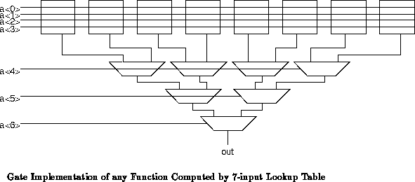
Conversely, by construction, we can show that any function computed by the
input lookup table can be computed with
gate
evaluations. As suggested in Figure
, we can use
gates to select the correct functional value based
on the low four bits of the address. We then build a binary mux reduction
tree to select the final output based on the remaining address bits. This
tree requires
muxes. Together, the
gates compute any function computable by the
-input lookup table.
An input by one output table lookup can thus provide between
and
gate evaluations per
cycle for the most complicated
input functions. Since the bounds are
essentially a factor of two apart, we can approximate the peak as
gate evaluations per cycle. If the table is
bits wide, the table provides at most
times as many gate evaluations.
Putting all this together, we get:
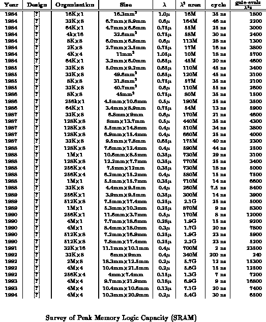
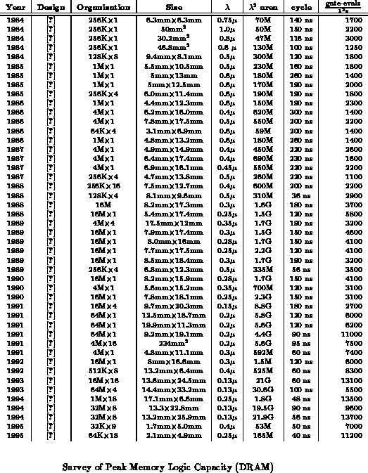
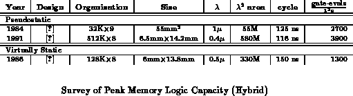
Tables ,
and
reviews memory implementations, showing
the peak functional density for each memory array. For the most complex
functions, memories provide the highest capacity of any general-purpose
architecture. For less complex operations, however, memories are
inefficient, yielding very little of their potential capacity.
For example, an 8-bit add operation with carry output requires 16
gate evaluations. Performed in a memory, such as a 9-bit
version of the 64K
18 memory from [SMK +94], this provides
only
. The
inefficiency of the memory-based adder increases with operand size since
the number of gate evaluations in an
-bit add increases as
whereas
the memory area increases as
.
For all the memories listed, the capacity is based on continuous cycles
of random access. In particular, nibble, fast page, or synchronous access
in DRAMs is not exploited. For example, [TNK +94] achieves
13,500 on random access.
In sequential access mode, the part can output 18 bits every 8ns. For
large sequential access, this means an effective cycle time of 8ns instead
of the 48ns quoted -- a factor of six improvement in cycle time and
capacity. Used in this mode, the peak performance is
81,000
.
It is also worth noting that, unlike processors, the capacity of memories has increased over time. This is likely due to:
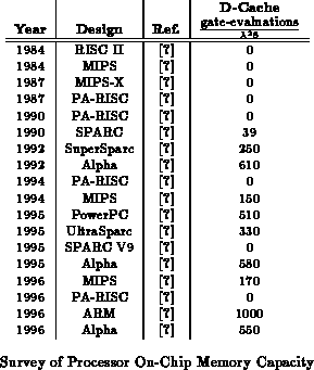
Modern processors actually dedicate a significant portion of their
area to memory. Table summarizes the peak
capacity the processor can extract by using table lookups in its D-cache.
The area used in calculating this capacity is the entire processor for the
processors listed in Table
. This peak capacity
can be thought of as the peak capacity one could extract from each load
operation when using the on-chip D-cache for table lookup operations.
Field-Programmable Gate Arrays (FPGAs) are composed of a collection of programmable gates embedded in a programmable interconnect. Programmable gates are often implemented using small lookup tables. The small lookup tables with programmable interconnect allow one to take advantage of the structure inherent in many computations to reduce the amount of memory and space required to implement a function versus the full memory arrays of the previous section. Ultimately, this allows FPGA space required for an application to scale with the complexity of the application rather than scaling exponentially in the manner of pure memories.
For pedagogical purposes, we consider an FPGA composed of:
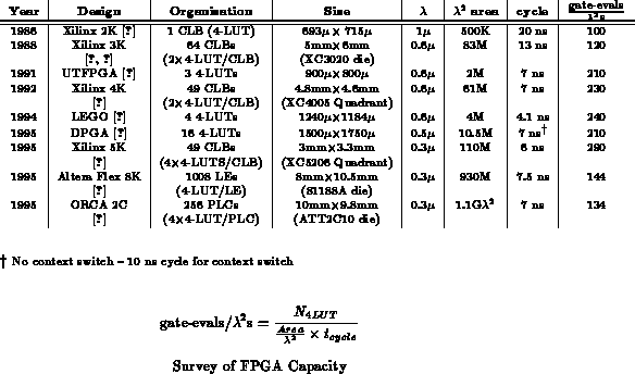
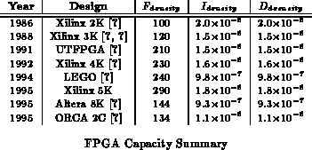
Running at full capacity and minimum operating cycle, the FPGA
provides gate evaluations per cycle. Modern FPGAs
can hold on the order of 2000 4-LUTs and run at cycle times on the order of
5-10ns. Table
computes the normalized capacity
provided by a few representative FPGAs. From these numbers we see that an
FPGAs provide a peak capacity on the order of
200-300
.
FPGA capacity has not change dramatically over time, but the sample size is small. There is a slight upward trend which is probably representative of the relative youth of the architecture.
This peak, too, is not achievable for every application. Some effects which may prevent an application from achieving this peak include:
As one example of pipelining, i/o, and functionality limitations,
DEC's Programmable Active Memories ran from 15-33MHz for several
application [BRV92]. At these rates, the peak
functional density extracted from the XC3090's employed was
13-26 , only
about 10-20% of the potential functional density.
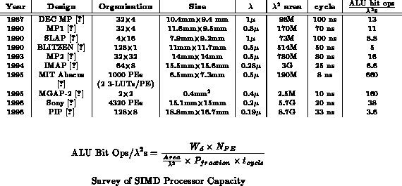
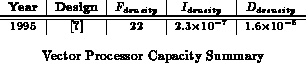
Single-Instruction, Multiple-Data (SIMD) machines are composed of a number of processing elements performing identical operations on different data items. Vector processors perform identical operations on a linear ensemble of data items. At a pedagogical level vector processors are essentially SIMD processors, though in practice the two architectures have traditionally been optimized for different usage scenarios.
For pedagogical purposes, we consider a SIMD/Vector array composed of:
The SIMD/Vector array provides provides a peak of ALU bit operations per cycle or
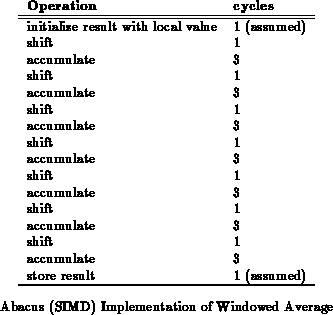
gate-evaluations per cycle. Abacus, a modern, fine-grained
SIMD array, supports 1000 1-bit PEs and can operate at 125MHz. Abacus thus
provides 660
.
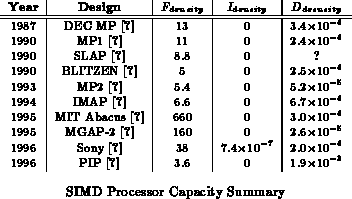
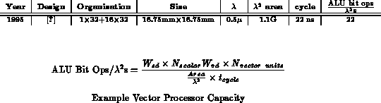
Table
computes the normalized capacity provided by
several SIMD arrays of varying granularity, and Table
shows the composition of a modern vector microprocessor.
SIMD/Vector arrays only achieve their peak capacity when every PE/VU is computing a useful logic operation on every cycle. Limitations to achieving this peak include:
Flynn [Fly72] summarizes some of the limitations associated with SIMD processing.
Multimedia processors are a recent hybrid of microprocessors, DSP, and Vector/SIMD processors. Aimed at processing video, graphics, and sound, these processors support efficient operation on data of various grain sizes by segmenting up their wide-word ALUs to provide SIMD parallel operation on the bytes within the word. This segmentation combats the increasing inefficiency associated with processing small data values on wide-word processors.
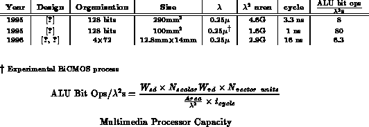
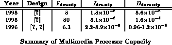
From Table , we see the CMOS multimedia
processor have the same peak functional density as processors. The major
difference is that the segmentation allows these processor to operate on
16-bit and byte-wide data without discarding a factor of 4-8
in
performance. Of course, this is true only as long as these finer-grained
operations can be performed efficiently in a SIMD manner.
The BiCMOS multimedia processor promised by MicroUnity would have a significantly higher performance density by exploiting a novel process. The comparison between their architecture in CMOS and BiCMOS makes it clear that this functional density advantage comes primarily from the process and not from the architecture.
Like FPGAs, multicontext FPGAs are composed of a collection of programmable gates embedded in a programmable interconnect. Unlike FPGAs, multicontext devices store several configurations for the logic and the interconnect on the chip. The additional area for the extra contexts decreases functional density, but it increases functional diversity by allowing each LUT element to perform several different functions.
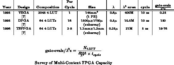
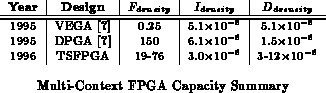
Table summarizes the capacities of some experimental,
multiple-context FPGAs. Like FPGAs, these devices may suffer from limited
interconnect or application pipelining limits. The additional context
memory makes them less susceptible to functionality limits than traditional
components. Chapter
details the usage of multicontext devices
including their relative capacity yield compared to single context devices.
Contemporary MIMD processors have largely been built from collections of microprocessors. As such, the functional density of these multiprocessors is certainly no larger than that of the microprocessors employed for the compute nodes. Since these machines typically require additional components for routing between processor and to connect processors into the routing network, the average functional density is actually much lower.
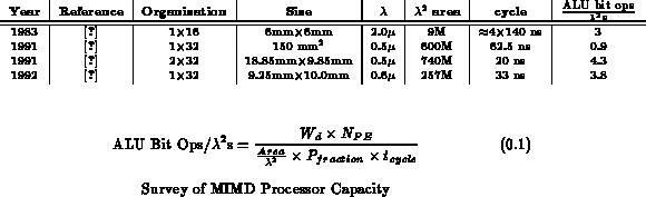
Table samples a few processors which were
designed explicitly for multiprocessor implementation. These processor
integrate the basic network interface and, in some cases, a portion of the
routing network, onto the device. While the sample size is too small to
draw any strong conclusions, the highest capacity implementations show only
about half the functional density of the microprocessors we reviewed
in Section
.
Reconfigurable ALUs are composed of a collection of coarse-grain ALUs embedded in a programmable interconnect. Their word orientation and limitation to ALU operations distinguishes them from FPGAs.
For pedagogical purposes, a reconfigurable ALU contains:
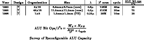
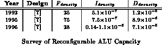
Running at full capacity and minimum operating cycle, the
reconfigurable ALU provides ALU bit
operations per cycle. Experimental reconfigurable ALUs achieve
roughly 50 ALU bit operations/
.
Like a processor D-cache, the memory on MATRIX can be used as a
large lookup table. Using the MATRIX 2568 memory for function
lookup, MATRIX can achieve up to
440 4-LUT gate-evaluations/
.
Like processor, reconfigurable ALUs may suffer lower yield due to:
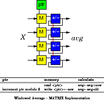
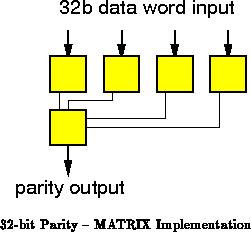
Table summarizes the observed
computational densities for the general-purpose architecture classes
reviewed in this section.
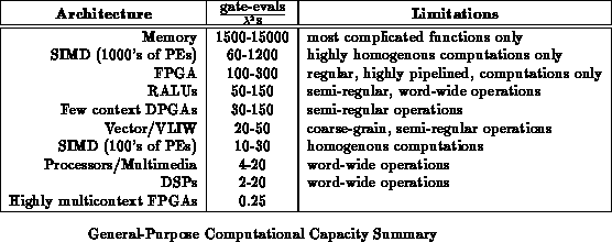
Memories provide the highest programmable capacity of any of the devices reviewed. However, they only yield this capacity on the most complex functions -- those whose complexity is, in fact, exponential in the number of input bits. The capacity they provide is not robust in the face of less complex tasks.
Reconfigurable devices provide the highest general-purpose capacity
which can be deployed to application needs. Unlike memories capacity
consumption scales along with problem complexity. Their peak performance
is 10 all non-reconfigurable architectures, with the exception of
large, well engineered SIMD arrays. Fine-grained devices, such as FPGAs,
are robust to grain-size variation, as well. Reconfigurable architectures
are not, however, robust to tasks with functional diversity larger than the
aggregate device capacity. Multicontext devices, such as the DPGA,
sacrifice a portion of the peak FPGA capacity density to partially mitigate
this problem -- providing support for much higher on chip functional
diversity.
Large SIMD or vector arrays have high peak performance because they ammortize a single stream of instruction control, bandwidth, and memory among a large number of active computing elements. They handle high diversity with the ability to issue a new instruction on each cycle. However, they require very large granularity operations in order to efficiently use the computational resources in the array.
Processors are robust to high functional diversity, but achieve this
robustness at a large cost in available capacity -- 10 below
reconfigurable devices. They also give up fine-grain control of
operations, creating a potential for another 10
loss in performance
when irregular, fine-grained operations are required. Vector and VLIW
structures provide slightly higher capacity density for very stylized usage
patterns, but are less robust to tasks which deviate from their stylized
control paradigm.
Here we see distinctions in granularity, operation diversity, and yieldable
capacity. The key issues we used to classify architectures was the way the
devices store and distribute instructions to processing elements.
Characterizing instructions and interconnect issues with a focus on
RP-space is the goal of Part .