Previous: New Architectures Up: New Architectures Next: Dynamically Programmable Gate Arrays with Input Registers
In Chapter we demonstrated that if we settle on a
single word width,
, we can select a robust context depth,
, such
that the area required to implement any task on the architecture with fixed
is at most 2
the area of using an architecture with optimal
. Further, for single bit granularities,
, the model predicted a
robust context depth
. In contrast, the primary, conventional,
general-purpose devices with independent, bit-level control over each
bit-processing unit are Field-Programmable Gate Arrays (FPGAs), which have
. Our analysis from Chapter
suggests that we can often
realize more compact designs with multicontext devices.
Figure
shows the yielded efficiency of a 16-context,
single-bit granularity device for comparison with
Figure
, emphasizing the broader range of efficiency
for these multicontext devices.

In this chapter, we introduce Dynamically Programmable Gate Arrays (DPGAs), fine-grained, multicontext devices which are often more area efficient than FPGAs. The chapter features:

The DPGA is a multicontext (), fine-grained (
), computing
device. Initially, we assume a single control stream (
). Each
compute and interconnect resource has its own, small, memory for describing
its behavior (See Figure
). These instruction
memories are read in parallel whenever a context (instruction) switch is
indicated.
The DPGA exploits two facts:

To illustrate the issue, consider the task of converting an ASCII
Hex digit into binary. Figure describes the basic computation
required. Assuming we care about the latency of this operation, a mapping
which minimizes the critical path length using SIS [SSL +92] and
Chortle [Fra92] has a path length of 3 and requires 21
4-LUTs. Figure
shows the LUT mapping both in
equations and circuit topology.


The multicontext LUT is slightly larger due to the extract
contexts. Two additional contexts add 160K to the LUT area,
making for
. The multicontext
implementation requires:
In contrast, a non-pipelined, single-context implementation would require
LUTs, for an area of:
If we assume that we can pipeline the configuration read,
the multicontext device can achieve comparable delay per LUT evaluation to
the single context device. The total latency then is 21 ns, as before.
The throughput at the 7 ns clock rate is 48 MHz. If we do not pipeline the
configuration read, as was the case for the DPGA prototype
(Section ), the configuration read adds another 2.5 ns
to the LUT delay, making for a total latency of 28.5 ns and a throughput of
35 MHz.
In an ideal packing, a computation requiring active
compute elements and
total 4-LUTs, can be implemented in area:
Equation is a simplification of our area model
(Equation
). Using the typical values suggested in
the previous chapter:
In practice, a perfect packing is difficult to achieve due to connectivity
and dependency requirements such that configuration
memories are required. In the previous example, we saw
for
due to retiming and packing
constraints. In fact, with the model described so far, retiming
requirements prevent us from implementing this task on any fewer than 12
active LUTs. Retiming requirements are one of the main obstacles to
realizing the full, ideal benefits. We will see retiming effects more
clearly when we look at circuit benchmarks in
Section
.
Several hardware logic simulator have been built which share a similar execution model to the DPGA. These designs were generally motivated to reduce the area required to emulate complex designs and, consequently, took advantage of the fact that task descriptions are small compared to to their physical realizations in order to increase logic density.
The Logic Simulation Machine [BLMR83], and later, the Yorktown
Simulation Engine (YSE) [Den82] were the earliest such hardware
emulators. The YSE was built out of discrete TTL and MOS memories,
requiring hundreds of components for each logic processor. Processors had
an 8K deep instruction memory (), 128 bit instructions
(
,
once processor-to-processor interconnect
is included) and produced two results per cycle (
). The YSE design
supported arrays of up to 256 processors (
), with a single
controller (
) running the logic processors in lock step, and a
full 256
256, 2-bit wide crossbar (
).
The Hydra processor which Arkos Design's developed for their Pegasus
hardware emulator is a closer cousin to the DPGA
[Mal94]. They integrate 32, 16-context, bit
processors on each Hydra chip (,
,
). The logic
function is an 8-input NAND with programmable input inversions.
VEGA uses 1K-2K context memories to achieved a 7 logic description
density improvement over single context FPGAs. At
, VEGA is
optimized to be efficient for very large ratios,
, and
can be quite inefficient for regular, high-throughput tasks. With
, and a separate controller per processor
(
), Equation
predicts a
VEGA processing element will have
, which is about 8.5
smaller than the 2048
single context processing elements which it emulates -- so the area savings
realized by VEGA is quite consistent with our area model developed in
Chapter
.
Hydra and VEGA were developed independently and concurrently to the DPGA, which was first described in [BDK94].
Dharma [Bha93][BCK93] was designed to solve the FPGA routing
problem. Logic is evaluated in strict levels similar to the scheme used
for circuit evaluation in Section with one
gate-delay evaluation per cycle. Dharma is based on a few, monolithic
crossbars (
) which are reused at each level of logic. Once gates have
been assigned to evaluation levels, the full crossbar makes placement and
routing trivial. While this arrangement is quite beneficial for small
arrays, the scaling rate of the full crossbar makes this scheme less
attractive for large arrays,
, as we saw in Section
.
DPGAs, as with any general-purpose computing device supporting the
rapid selection among instructions, are beneficial in cases where only a
limited amount of functionality is needed at any point in time, and where
it is necessary to rapidly switch among the possible functions needed.
That is, if we need all the throughput we can possibly get out of a single
function, as in the fully-pipelined ASCII HexBinary converter
in Section
, then an FPGA, or other purely spatial
reconfigurable architecture will handle the task efficiently. However,
when the throughput requirements from a function are limited or the
function is needed only intermittently, a multicontext device can provide a
more efficient implementation. In this section, we look at several,
commonly arising situations where multicontext devices are preferable to
single-context devices, including:
Often the system environment places limits on the useful throughput for a subtask. As we saw in the introduction to this chapter, when the raw device supports a higher throughput than that required from the task, we can share the active resources in time among tasks or among different portions of the same task.
Most designs are composed of several sub-components or sub-tasks, each
performing a task necessary to complete the entire application (See
Figure ). The overall performance of the design
is limited by the processing throughput of the slowest device. If the
performance of the slowest device is fixed, there is no need for the other
devices in the system to process at substantially higher throughputs.

In these situations, reuse of the active silicon area on the
non-bottleneck components can improve performance or lower costs. If we
are getting sufficient performance out of the bottleneck resource, then we
may be able to reduce cost by sharing the gates on the non-bottleneck
resources between multiple ``components'' of the original design (See
Figure ). If we are not getting sufficient performance
on the bottleneck resource and its task is parallelizable, we may be able
to employ underused resources on the non-bottleneck components to improve
system performance without increasing system cost (See
Figure
).


When data throughput is limited by I/O bandwidth, we can reuse the internal resources to provide a larger, effective, internal gate capacity. This reuse decrease the total number of devices required in the system. It may also help lower the I/O bandwidth requirements by grouping larger sets of interacting functions on each IC.
Some designs are limited by latency not throughput. Here, high throughput may be unimportant. Often it is irrelevant how quickly we can begin processing the next datum if that time is shorter than the latency through the design. This is particularly true of applications which must be serialized for correctness ( e.g. atomic actions, database updates, resource allocation/deallocation, adaptive feedback control).
By reusing gates and wires, we can use device capacity to implement these latency limited operations with less resources than would be required without reuse. This will allow us to use smaller devices to implement a function or to place more functionality onto each device.
Some computations have cyclic dependencies such that they cannot continue until the result of the previous computation is known. For example, we cannot reuse a multiplier when performing exponentiation until the previous multiply result is known. Finite state machines (FSMs) also have the requirement that they cannot begin to calculate their behavior in the next state, until that state is known. In a purely spatial implementation, each gate or wire performs its function during one gate delay time and sits idle the rest of the cycle. Active resource reuse is the most beneficial way to increase utilization in cases such as these.
Another characteristic of finite state machines is that the computational task varies over time and as a function of the input data. At any single point in time, only a small subset of the total computational graph is needed. In a spatial implementation, all of the functionality must be implemented simultaneously, even though only small subsets are ever used at once. This is a general property held by many computational tasks.
Many tasks may perform quite different computations based on the kind of data they receive. A network interface may handle packets differently based on packet type. A computational function may handle new data differently based on its range. Data objects of different types may require widely different handling. Rather than providing separate, active resources for each of these mutually exclusive cases, a multicontext device can use a minimum amount of active resources, selecting the proper operational behavior as needed.
Multicontext devices are specifically tailored to the cases where we need a limited amount of active functionality at any point in time, but we need to be able to select or change that functionality rapidly. This rapid switching is necessary to obtain reasonable performance for the kinds of applications described in this section. This requirement makes reconfigurations from a central memory pool, on or off chip, inadequate.
In this section, we draw out this point, reviewing the application domains identified in the previous section. We also look at cases where one can get away without multicontext devices. At the end of this section, we articulate a reconfiguration rate taxonomy which allows us to categorize both device architectures and applications.
From the above, we see three cases for configuration management based on the rate at which the task requires distinct pieces of functionality and the rate at which it is efficient to change the configuration applied to the active processing elements:
We can further subdivide configuration management capabilities of architecture and application requirements based on whether they can take advantage of limited bandwidth configuration edits:
Jeremy Brown, Derrick Chen, Ian Eslick, and Edward Tau started a first-generation prototype DPGA prototype while they were taking MIT's introductory VLSI course (6.371) during the Fall of 1994. The chip was completed during the Spring of 1995 with additional help from Ethan Mirsky. Andre DeHon helped the group hash out the microarchitecture and oversaw the project. The prototype was first presented publicly in [TEC +95]. A project report containing lower level details is available as [BCE +94].
In this section, we describe this prototype DPGA implementation. The design represents a first generation effort and contains considerable room for optimization. Nonetheless, the design demonstrates the viability of DPGAs, underscores the costs and benefits of DPGAs as compared to traditional FPGAs, and highlights many of the important issues in the design of programmable arrays. The fabricated prototype did have one timing problem which prevented it from functioning fully, but our post mortem analysis suggests that the problem is easily avoidable.
Our DPGA prototype features:
We begin by detailing our basic DPGA architecture in
Section . Section
provides highlights from our implementation including key details on our
prototype DPGA IC. In Section
, we describe several
aspects of the prototype's operation. Section
extracts a DPGA area model based on the prototype implementation.
Section
closes out this section on the DPGA
prototype by summarizing the major lessons from the effort.

Figure depicts the basic architecture for this DPGA. Each
array element is a conventional 4-input lookup table (4-LUT). Small
collections of array elements, in this case 4
4 arrays, are grouped
together into subarrays. These subarrays are then tiled to compose
the entire array. Crossbars between subarrays serve to route inter-subarray
connections. A single, 2-bit, global context identifier is distributed
throughout the array to select the configuration for use. Additionally,
programming lines are distributed to read and write configuration memories.


This leaf topology is limited to moderately small subarrays since it ultimately does not scale. The row and column widths remains fixed regardless of array size so the horizontal and vertical interconnect would eventually saturate the row and column channel capacity if the topology were scaled up. Additionally, the delay on the local interconnect increases with each additional element in a row or column. For small subarrays, there is adequate channel capacity to route all outputs across a row and column without increasing array element size, so the topology is feasible and desirable. Further, the additional delay for the few elements in the row or column of a small subarray is moderately small compared to the fixed delays in the array element and routing network. In general, the subarray size should be carefully chosen with these properties in mind.

While the nearest neighbor interconnect is sufficient for the 33
array in the prototype, a larger array should include a richer
interconnection scheme among subarrays. At present, we anticipate that a
mesh with bypass structure with hierarchically distributed interconnect
lines will be appropriate for larger arrays.

The DPGA prototype is targeted for a 1 drawn, 0.85
effective gate
length CMOS process with 3 metal layers and silicided polysilicon and
diffusion. Table
highlights the
prototype's major characteristics. Figure
shows
the fabricated die, and Figure
shows a closeup of the
basic subarray tile containing a 4
4 array of LUTs and four
inter-subarray crossbars. Table
summarizes the areas
for the constituent parts.
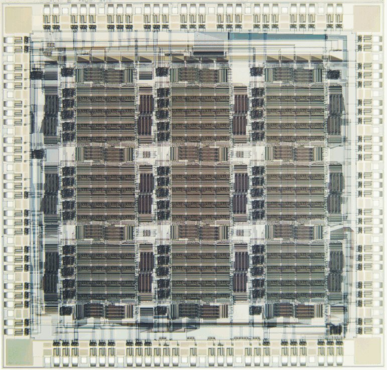


Table breaks down the chip area by consumers.
In Table
, configuration memory is divided between
those supporting the LUT programming and that supporting interconnect.
All together, the configuration memory accounts for 33% of the total die
area or 40% of the area used on the die. The network area, including
local interconnect, wiring, switching, and network configuration area
accounts for 66% of the die area or 80% of the area actually used on the
die. Leaving out the configuration memory, the fixed portion of the
interconnect area is 45% of the total area or over half of the active die
area.

From the start, we suspected that memory density would be a large
determinant of array size. Table demonstrates this
to be true. In order to reduce the size of the memory, we employed a 3
transistor DRAM cell design as shown in Figure
. To keep
the aspect ratio on the 4
32 memory small, we targeted a very narrow
DRAM column (See Figure
).

Unfortunately, this emphasis on aspect ratio did not allow us to
realize the most area efficient DRAM implementation (See
Table ). In particular, our DRAM cell was
7.6
19.2
, or almost 600
. A tight DRAM should
have been 75-80
, or about 300
. Our tall and thin DRAM
was via and wire limited and hence could not be packed as area efficiently
as a more square DRAM cell.

One key reason for targeting a low aspect ratio was to balance the number of interconnect channels available in each array element row and column. However, with 8 interconnect signals currently crossing each side of the array element, we are far from being limited by saturated interconnect area. Instead, array element cell size is largely limited by memory area. Further, we route programming lines vertically into each array element memory. This creates an asymmetric need for interconnect channel capacity since the vertical dimension needs to support 32 signals while the horizontal dimension need only support a dozen memory select and control lines.
For future array elements we should optimize memory cell area with less concern about aspect ratio. In fact, the array element memory can easily be split in half with 16 bits above the fixed logic in the array element and 16 below. This rearrangement will also allow us to distribute only 16 programming lines to each array element if we load the top and bottom 16 bits separately. This revision does not sacrifice total programming bandwidth if we load the top or bottom half of a pair of adjacent array elements simultaneously.

Table further decomposes memory area
percentages by function. We have already noted that a tight DRAM cell
would be half the area of the prototype DRAM cell and an SRAM cell would be
twice as large. Using these breakdowns and assuming commensurate savings
in proportion to memory cell area, the tight DRAM implementation would save
about 7% total area over the current design. An SRAM implementation would
be, at most, 15% larger. In practice, the SRAM implementation would
probably be only 5-10% larger for a 4-context design since the refresh
control circuitry would no longer be needed. Of course, as one goes to
greater numbers of contexts, the relative area differences for the memory
cells will provide a larger contribution to overall die size.
The memory in the fabricated prototype suffered from a timing
problem due to the skew between the read precharge enable and the internal
write enable. As shown in Figure , the read bus is
precharged directly on the high edge of the clock signal clk. The
internal write enable, iwe, controls write-back during refresh.
iwe and the write enable signals, we<4:0>, are generated by the
local decoder and driven across an entire row of four array elements in a
subarray, which makes for a 128-bit wide memory. Both iwe and
we<4:0> are pipelined signals which transition on the rising edge of
clk. On the rising edge of clk, we have a race between the
turn on of the precharge transistor and the turn off of iwe and
we<4:0>. Since clk directly controls the precharge transistor,
precharge begins immediately. However, since iwe and
we<4:0> are registered, it takes a clock-to-q delay before they can
begin to change. Further, since there are 128 consumers spread across
1100
, the signal propagation time across the subarray is non-trivial.
Consequently, it is possible for the precharge to race through write
enables left on at the end of a previous cycle and overwrite memory. This
problem is most acute for the memories which are farthest from the local
decoders.
Empirically, we noticed that the memories farthest from the local decoder lost their values after short time periods. In the extreme cases of the input and output pads, which were often very far from their configuration memories, the programmed values were overwritten almost immediately. The memories closer to the local decoder were more stable. The array elements adjacent to the decoders were generally quite reliable. After identifying this potential failure mode, we simulated explicit skew between clk and the write enables in SPICE. In simulation, the circuit could tolerate about 1.5 ns of skew between clk and the write enables before the memory values began to degrade.
We were able to verify that refresh was basically operational. By continually writing to single context, we can starve other contexts from ever refreshing. When we forced the chip into this mode, data disappeared from the non-refreshed memories very quickly. The time constant on this decay was significantly different from the time constants observed due to the timing decay giving us confidence that the basic refresh scheme worked aside from the timing skew problem.
Obviously, the circuit should have been designed to tolerate this
kind of skew. A simple and robust solution would have been to disable the
refresh inverter or the writeback path directly on to avoid simultaneously enabling both the precharge and writeback
transistors. Alternately, the precharge could have been gated and
distributed consistently with the write enables.

To keep configuration memory small, the crossbar enables were
stored encoded in configuration memory then decoded for crossbar control.
The same 432 memory used for the array element was used to control
each 16
8 crossbar. Note that the entire memory is 128K
.
The crossbar itself is 535K
, making the pair 660K
.
Had we not encoded the crossbar controls, the crossbar memory alone would
have occupied 512K
before we consider the crossbar itself. This
suggests that the encoding was marginally beneficial for our four context
case, and would be of even greater benefit for greater numbers of contexts.
For fewer contexts, the encoding would not necessarily be beneficial.

Table summarizes the key timing estimates for the DPGA
prototype at the slow-speed and nominal process points. As shown, context
switches can occur on a cycle-by-cycle basis and contribute only a few
nanoseconds to the operational cycle time. Equation
relates
minimum achievable cycle time to the number of LUT delays,
, and
crossbar crossings,
in the critical path of a design.
These estimates suggest a heavily pipelined design which placed only one
level of lookup table logic () and one
crossbar traversal (
) in each pipeline stage could achieve 60-100MHz
operation allowing for a context switch on every cycle. Our prototype,
however, does not have a suitably aggressive clocking, packaging, or i/o
design to actually sustain such a high clock rate. DRAM refresh
requirements force a minimum operating frequency of 5MHz.
Two areas for pipelining are worth considering. Currently, the
context memory read time happens at the beginning of each cycle. In many
applications, the next context is predictable and the next context read can be
pipelined in parallel with operation in the current context. This
pipelining can hide the additional latency, . Also, notice that
the inter-subarray crossbar delay is comparable to the LUT plus local
interconnect delay. For aggressive implementations, allowing the
non-local interconnect to be pipelined will facilitate small microcycles
and very high throughput operation. Pipelining both the crossbar routing
and the context reads could potentially allow a 3-4 ns operational cycle.
The only method of inter-context communication for the prototype is
through the array element output register. That is, when a succeeding
context wishes to use a value produced by the immediately preceding
context, we enable the register output on the associated array element in
the succeeding context (See Figure ). When the clock edge
occurs signaling the end of the preceding cycle, the signal value is
latched into the output register and the new context programming is read.
In the new context, the designated array element output now provides the
value stored from the previous context rather than the value produced
combinationally by the associated LUT. This, of course, makes the
associated LUT a logical choice to use to produce values for the new
context's succeeding context since it cannot be used combinationally in the
new context, itself.
In the prototype, the array element output register is also the only means of state storage. Consequently, it is not possible to perform orthogonal operations in each context and preserve context-dependent state.
Note that a single context which acts as a shift register can be used to snapshot, offload, and reload the entire state of a context. In an input/output minimal case, all the array elements in the array can be linked into a single shift register. Changing to the shift register context will allow the shift register to read all the values produced by the preceding context. Clocking the device in this context will shift data to the output pin and shift data in from the input pin. Changing from this context to an operating context which registers the needed inputs will insert loaded values for operation. Such a scheme may be useful to take snapshots during debugging or to support context switches where it is important to save state. If only a subset of the array elements in the array produce meaningful state values, the shift register can be built out of only those elements. If more input/output signals can be assigned to data onload and offload, a parallel shift register can be built, limiting the depth and hence onload/offload time.
The context memory typically gets very stylized usage. For any single memory, writes are infrequent. Common usage patterns are to read through all the contexts or to remain in one context for a number of cycles. As such the usage pattern is complementary to DRAM refresh requirements.
Using the prototype areas, we can formulate a simplified model for
the area of an -context DPGA array element.
From the prototype:
Based on this area model, our robust context point,
, is 45, 23, and 11,
respectively for each of the various memory implementations.
The prototype demonstrates that efficient, dynamically programmable gate
arrays can be implemented which support a single cycle, array-wide context
switch. As noted in Chapter and the introduction to this
chapter, when the instruction description area is small compared to the
active compute and network area, multiple context implementations are more
efficient than single context implementations for a large range of
application characteristics. The prototype bears out this relationship
with the context memory for each array element occupying at least an order
of magnitude less area than the fixed logic and interconnect area. The
prototype further shows that the context memory read overhead can be small,
only a couple of nanoseconds.
The prototype has room for improvement in many areas:
One large class of workloads for traditional FPGAs is
conventional circuit evaluation. In this section, we look at circuit
levelization where traditional circuits are automatically mapped into
multicontext implementations. In latency limited designs
(Section ), the DPGA can achieve comparable
delays in less area. In applications requiring limited task throughput
(Section
), DPGAs can often achieve the
required throughput in less area.
Levelized logic is a CAD technique for automatic temporal pipelining of existing circuit netlists. Bhat refers to this technique as temporal partitioning in the context of the Dharma architecture [Bha93]. The basic idea is to assign an evaluation context to each gate so that:

For sake of illustration, Figure shows a
fraction of the ASCII
Hex binary circuit extracted from
Figure
. The critical paths ( e.g.
c<1
i8
i15
o<1>) is three
elements long. Spatially implemented, this netlist evaluates a 6 gate
function in 3 cycles using 6 physical gates. In three cycles, these three
gates could have provided
gate evaluations, so we
underutilize all the gates in the circuit. The circuit can be fully
levelized as shown in Figure
(
= {i1,i4,i7,i8},
= {i15},
= {o<1>}) or partially levelized combining the
final two stages (
= {i1,i4,i7,i8},
= {i15,o<1>}). If
the inputs are held constant during evaluation, we need only four LUTs to
evaluate either case. In this case, if the inputs are not held constant,
we will need two additional LUTs in
for retiming so there is no
benefit to multicontext evaluation. However, as we saw in
Section
, for the whole circuit, even with retiming, the
total number of LUTs needed for levelized evaluation is smaller than the
number needed in a fully spatial implementation.
Recall also from Section , that grouping is one of the
limits to even levelization. When there is slack in the circuit
network, the slack gives us some freedom in the context placement
for components outside of the critical path. In general, this slack should
be used to equalize context size, minimizing the number of active LUTs
required to achieve the desired task latency or throughput. As we see in
both this subcircuit and the full circuit, signal retiming requirements
also serve to increase the number of active elements we need in each
evaluations level.
As noted in Section , many tasks are latency
limited. This could be due to data dependencies, such that the output
from the previous evaluation must be available before subsequent
evaluation may begin. Alternately, this subtask may be the latency
limiting portion of some larger computational task. Further, the task may
be one where the repetition rate is not hight, but the response time is
critical. In these cases, multicontext evaluation will allow
implementations with fewer active LUTs and, consequently, less
implementation area.
We use the MCNC circuit benchmark suite to characterize the benefits of multicontext evaluation. Each benchmark circuit is mapped to a netlist of 4-LUTs using sis [SSL +92] for technology independent optimization and Chortle [Fra92] [BFRV92] for LUT mapping. Since we are assuming latency is critical in this case, both sis and Chortle were run in delay mode. No modifications to the mapping and netlist generation were made for levelized computation.
LUTs are initially assigned to evaluation contexts randomly without
violating the circuit dataflow requirements. A simple, annealing-based
swapping schedule is then used to minimize total evaluation costs.
Evaluation cost is taken as the number of 4-LUTs in the final mapping
including the LUTs added to perform retiming.
Table shows the circuits mapped to a two-context DPGA, and
Table
, a four-context DPGA.
Table
shows the full levelization case -- that is
circuits are mapped to an
-context DPGA, where
is equal to the
number of LUT delays in the circuit's critical path.
The tables break out the number of active LUTs in the multicontext
implementations to show the effects of signal retiming requirements.


From the mapped results, we see a 30-40% overall area reduction using multicontext FPGAs, with some designs achieving almost 50%. For this collection of benchmark circuits, which has an average critical path length of 5-6 4-LUT delays, a four context DPGA gives the best, overall, results. Note that retiming requirements for these circuits dictates that each context contain, on average, 50% of the LUTs in the original design. Without the retiming requirements, 60-70% area savings look possible without increasing evaluation path length.
In addition to task delay requirements, three effects are working together here to limit the number of contexts which are actually beneficial for for these circuits:


When the number of LUT delays in the path is not an even multiple of the number of contexts, it is not possible to allocate an even number of LUT delays to each context. For example, since the des circuit takes eight LUT delays to evaluate, a three context implementation will place three LUT delays in two of the three contexts and two LUT delays in the third. In a simple clocking scheme, each context would get the same amount of time. In the des case, that would be three LUT delays, making the total evaluation time nine LUT delays.
Changing contexts will add some latency overhead at least for
registering values during context switches. In the circuit evaluation
case, the next context is always deterministic and could effectively be
pipelined in parallel with evaluation of the previous context. From the DPGA
prototype, we saw that LUT-to-LUT delay was roughly 6 ns and the context
read was 2.5 ns. Register clocking overhead is likely to be on the order
of 1 ns. This gives:
In the pipelined read case, we add 1 ns per context switch or at most
% delay to the critical path.
In the non-pipelined read case, we add 2.5 ns per context switch, or at most
% delay to the critical path.
The area for the multicontext implementation is smaller and the number of LUTs involved is smaller. As a result, the interconnect traversed in each context may be more physically and logically local, thus contributing less to the LUT-to-LUT delay.
The results presented in this section are based on:
In Section , we saw that system and
application requirements often limit the throughput required out of each
individual subtask or circuit. When throughput requirements are limited,
we can often meet the throughput requirement with fewer active LUTs than
design LUTs, realizing a smaller and more economical implementation.
To characterize this opportunity we again use the MCNC circuit benchmarks. sis and Chortle are used for mapping, as before. Since we are assuming here that the target criteria is throughput, both sis and Chortle are run in delay mode. As before, no modifications to the mapping and netlist generation are made.
For baseline comparison in the single-context FPGA case, we insert
retiming registers in the mapped design to achieve the required throughput.
That is, if we wish to produce a new result every LUT delays, we add
pipelining registers every
LUTs in the critical path. For example, if
the critical path on a circuit is 8 LUT delays long and the desired
throughput is one result ever 2 LUT delays, we break the circuit into four
pipeline stages, adding registers every 2 LUT delays in the original
circuit. We use a simple annealing algorithm to assign non-critical path
LUTs in order to minimize the number of retiming registers which must be
added to the design.
Similarly, we divide the multicontext case into separate spatial pipeline stages such that the path length between pipeline registers is equal to the acceptable period between results. The LUTs within a phase are then evaluated in multicontext fashion using the available contexts. Again, if the critical path on a circuit is 8 LUT delays long and the desired throughput is one result every 2 LUT delays, we break the circuit into four spatial pipeline stages, adding registers ever 2 LUT delays in the original circuit. The spatial pipeline stage is further subdivided into two temporal pipeline stages which are evaluated using two contexts. This multicontext implementation switches contexts on a one LUT delay period. Similarly, if the desired throughput was only one result every 4 LUT delays, the design would be divided into 2 spatial pipeline stages and up to 4 temporal pipeline stages, depending on the number of contexts available on the target device. The same annealing algorithm is used to assign spatial and temporal pipeline stages to non-critical path LUTs in a manner which minimizes the number of total design and retiming LUTs required in the levelized circuit.
As the throughput requirements diminish, we can generally achieve
smaller implementations. Unfortunately, as noted in the previous section
retiming requirements prevent us from effectively using a large number of
contexts to decrease implementation area. For the alu2 benchmark,
Table shows how LUT requirements vary with
throughput and Table
translates the LUT
requirements into areas based on the model parameters used in the previous
section. Figure
plots the areas from
Table
. Table
recasts the areas from Table
as ratios to the
the best implementation area at a given throughput. For this circuit, the
four or five context implementation is
45% smaller than the
single context implementation for low throughput requirements.


Tables through
highlight area ratios at three throughput points for the entire
benchmark set. For reference, Table
summarizes the number of mapped design LUTs and path lengths for the
netlists used for these experiments. We see that the 2-4 context
implementations are 20-30% smaller than the single context implementations
for low throughput requirements.


The results shown here are moderately disappointing. Retiming requirements prevent us from collapsing the number of active LUTs substantially as we go to deeper multicontext implementations. As with the previous section, the results presented in this section are based on our area model, the prototype DPGA architecture, and conventional circuit netlist mapping. More than in the previous section, the results here also depend upon the experimental temporal partitioning CAD software. Groupings into temporal and spatial pipelining stages are more rigid than necessary, so better packing may be possible with more flexible stage assignment. The retiming limitations identified here also motivate architectural modifications which we will see in the next chapter.
The retiming limitation we are encountering here arises largely from packing the circuit into a limited number of LUTs and serializing the communication of intermediate results. An alternate strategy would be to share a larger group of LUTs more coarsely between multiple subcircuits in a time-sliced fashion. That is, rather than trying to sequentialize the evaluation, we retain the full circuit, or a partially sequentialized version, and only invoke it periodically.
Considering again our alu2 example, for moderately low
throughput tasks, one context may hold the 169 mapped design LUTs, while
other contexts hold other, independent, tasks. A two context DPGA could
alternate switch between evaluating the alu2 example and some other
circuit or task. In this two context case, the amortized area would be:
Note that 81M
is smaller than the 91M
area which the
two context, non-interleaved implementation achieved
and smaller than the 84-85M
for the four and five context implementation
(Table
). Further interleaving can yield even
lower amortized costs. e.g.

This coarse-grain interleaving achieves a more ideal reduction in area:
Figure plots the area ratio
versus
.
Note that the ratio is ultimately bounded by the
ratio, which is roughly 10% for the
model parameters assumed throughout this section.
On the negative side,
As we noted in Sections
and
, the performance of a finite state machine is
dictated by its latency rather than its throughput. Since the next state
calculation must complete and be fed back to the input of the FSM before
the next state behavior can begin, there is no benefit to be gained from
spatial pipelining within the FSM logic. Temporal pipelining can be used
within the FSM logic to increase gate and wire utilization as seen in
Section
. Finite state machines, however,
happen to have additional structure over random logic which can be
exploited. In particular, one never needs the full FSM logic at any point
in time. During any cycle, the logic from only one state is active. In a
traditional FPGA, we have to implement all of this logic at once in order
to get the full FSM functionality. With multiple contexts, each context
need only contain a portion of the state graph. When the machine transitions
to a state whose logic resides in another context, we can switch contexts
making a different portion of the FSM active. National Semiconductor, for
example, exploits this feature in their multicontext programmable logic
array (PLA), MAPL [Haw91].
Figure shows a simple, four-state FSM for illustrative
purposes. The conventional, single-context implementation requires four
4-LUTs, one to implement each of Dout and NS1 and two to
calculate NS0. Figure
shows a two-context DPGA
implementation of this same FSM. The design is partitioned into two
separate circuits based on the original state variable S1. The two
circuits are placed in separate contexts and NS1 is used to select
the circuit to execute as appropriate. Each circuit only requires three
4-LUTs, making the overall design smaller than the flat, single context
implementation.


In the most extreme case, each FSM state is assigned its own
context. The next state computation simply selects the appropriate next
context in which to operate. Tables
and
show the reduction in area and path delay
which results from state-per-context multiple context implementation of the
MCNC FSM benchmarks. FSMs were mapped using mustang
[DMNSV88]. Logic minimization and LUT mapping were done with
espresso, sis, and Chortle. For single context FSM
implementations, both one-hot and dense encodings were synthesized and the
best mapping was selected. The multicontext FSM implementations use dense
encodings so the state specification can directly serve as the context
select. For multicontext implementations, delay and capacity are dictated
by the logic required for the largest and slowest state. On average, the
fully partitioned, multicontext implementation is 35-45% smaller that the
single context implementation. Many FSMs are 3-5
smaller.


From Tables and
,
the multicontext FSM implementations generally have one or two fewer logic
levels in their critical path than the single context implementations when
mapped for minimum latency. The multicontext implementations have an even
greater reduction in path length when mapped for minimum area.
The multicontext FSMs, however, require additional time to distribute the
context select and perform the multi-context read. i.e.
Recall from the prototype and
with a typical amount of switching. Properly
engineered, context distribution should take a few nanoseconds, which means
the multicontext and single-context implementations run at comparable
speeds when the multicontext implementation has one fewer LUT delays in its
critical path than the single-context implementation.
The capacity utilization and delay are often dictated by a few of
the more complex states. It is often possible to reduce the number of
contexts required without increasing the capacity required or increasing
the delay. Tables and
show the
cse benchmark partitioned into various numbers of contexts and
optimized for area or path delay, respectively. These partitions were
obtained by partitioning along mustang assigned state bits starting
with a four bit state encoding. Figures
and
plot the LUT count, area, and delay data
from the tables versus the number of contexts employed.


One thing we note from both the introductory example
(Figures and
) and the cse example is
that the full state-per-context case is not always the most area efficient
mapping. In the introductory example, once we had partitioned to two
contexts, no further LUT reduction could be realized by going to four
contexts. Consequently, the four context implementation would be larger
than the two context implementation owing to the deeper context memories.
In the cse example, the reduction in LUTs associated with going to
going from 8 to 11 or 11 to 16 contexts saved less area than the cost of
the additional context memories.
Tables
through
show the benchmark set mapped to
various multicontext implementations for minimum area. All
partitioning is performed along mustang state bits. For these
results, we examined all possible state bits along which to split and chose
the best set. On average across the benchmark set, the 8-context mapping
saves over 40% in area versus the best single-context case. The best
multicontext mapping is often 3-5
smaller than the best single
context mapping.


Tables
through
show the benchmark set mapped to
various numbers of context implementations with delay minimization as the
target. All partitioning is performed along mustang state bits. For
these results, we examined all possible state bits along which to split and
chose the best set. On average across the benchmark set, the 8 context
mapping are half the area of the best single-context case while achieving
comparable delay.


A memory and a state register can also be used to implement
finite-state machines. The data inputs and current state are packed
together and used as addresses into the memory, and the memory outputs
serve as machine outputs and next state outputs.
Figure shows a memory implementation of our simple FSM
example from Figures
and
.

Used for finite-state machines, the DPGA is a hybrid between a
purely gate (FPGA) implementation and a purely memory implementation. The
DPGA takes advantage of the memory to realize smaller, state-specific logic
than an FPGA which must implement all logic simultaneously. The DPGA uses
the restructurable interconnect in the array to implement next-state and
output computations out of gates. As we noticed in Section ,
the gate implementation allow the DPGA to exploit regularities in the
computational task. In this case, we avoid the necessarily exponential
area increase associated with additional inputs in a memory implementation,
the linear-log increase associated with additional states, and the linear
increase associated with additional outputs.
Assuming we could build just the right sized memory for a given
FSM, the area would be:
Table
summarizes the areas of the best
memory-based FSM implementations along with the areas for FPGA and
8-context DPGA implementations. The ``Min area'' column indicates the area
assuming a memory of exactly the right size is used, while the ``Memory
Area'' field shows the area for the smallest memory with an integral number
of address bits as shown in the ``organization'' column. When the total
number of state bits and input bits is less than 11, the optimal memory
implementations can be much smaller than the FPGA or DPGA implementation.
Above 11 input and state bits, the DPGA implementation is smaller. Since
the DPGA implementation size increases with task complexity rather than
number of inputs, while the memory implementation is exponential in the
number of inputs and state bits, the disparity grows substantially as the
number of inputs and state bits increase.

While demonstrated in the contexts of FSMs, the basic technique used here is fairly general. When we can predict which portions of a netlist, circuit, or computational task are needed at a given point in time, we can generate a more specialized design which only includes the required logic. The specialized design is often smaller and faster than the fully general design. With a multicontext component, we can use the contexts to hold many specialized variants of a design, selecting them as needed.
In the synthesis of computations, it is common to synthesize a controller along with datapaths or computational elements. The computations required are generally different from state to state. Traditional, spatial implementations must have hardware to handle all the computations or generalize a common datapath to the point where it can be used for all the computations. Multicontext devices can segregate different computational elements into different contexts and select them only as needed.
For example, in both dbC [GM93] and PRISM-II [AWG94] a general datapath capable of handling all of the computational subtasks in computation is synthesized alongside the controller. At any point in time, however, only a small portion of the functionality contained in the datapath is actually needed and enabled by the controller. The multicontext implementation would be smaller by folding the disparate logic into memory and reusing the same active logic and interconnect to implement them as needed.
With multiple, on-chip contexts, a device may be loaded with several
different functions, any of which is immediately accessible with minimal
overhead. A DPGA can thus act as a ``multifunction peripheral,''
performing distinct tasks without idling for long reconfiguration
intervals. In a system such as the one shown in Figure ,
a single device may perform several tasks. When used as a reconfigurable
accelerator for a processor ( e.g. [AS93]
[DeH94] [RS94]) or to implement a dynamic
processor ( e.g. [WH95]), the DPGA can support multiple
loaded acceleration functions simultaneously. The DPGA is more efficient
in these allocations than single-context FPGAs because it allows rapid
reuse of resources without paying the large idle-time overheads associated
with reconfiguration from off-chip memory.
In a data storage or transmission application, for instance, one may be limited by the network or disk bandwidth. A single device may be loaded with functions to perform:
Within a CAD application, such as espresso [RSV87], one needs to perform several distinct operations at different times, each of which could be accelerated with reconfigurable logic. We could load the DPGA with assist functions, such as:
Some classes of functionality are needed, occasionally but not continuously. In conventional systems, to get the functionality at all, we have to dedicate wire or gate capacity to such functions, even though they may be used very infrequently. A variety of data loading and unloading tasks fit into this ``infrequent use'' category, including:
In a multicontext DPGA, the resources to handle these infrequent cases can be relegated to a separate context, or contexts, from the ``normal'' case code. The wires and control required to shift in (out) data and load it are allocated for use only when the respective utility context is selected. The operative circuitry then, does not contend with the utility circuitry for wiring channels or switches, and the utility functions do not complicate the operative logic. In this manner, the utility functions can exist without increasing critical path delay during operation.
A relaxation algorithm, for instance, might operate as follows:

Figure shows a typical video coding pipeline ( e.g.
[JOSV95]). In a conventional FPGA implementation, we
would lay this pipeline out spatially, streaming data through the pipeline.
If we needed the throughput capacity offered by the most heavily pipelined
spatial implementation, that would be the design of choice. However, if we
needed less throughput, the spatially pipelined version would require the
same space while underutilizing the silicon. In this case, a DPGA
implementation could stack the pipeline stages in time. The DPGA can
execute a number of cycles on one pipeline function then switch to another
context and execute a few cycles on the next pipeline function (See
Figure
). In this manner, the lower throughput
requirement could be translated directly into lower device requirements.

This is the same basic organizational scheme used for levelized
logic evaluation (Section ). The primary
difference being that evaluation levels are divided according to
application subtasks.
This is a general schema with broad application. The pipeline design style is quite familiar and can be readily adapted for multicontext implementation. The amount of temporal pipelining can be varied as throughput requirements change or technology advances. As silicon feature sizes shrink, primitive device bandwidth increases. Operations with fixed bandwidth requirements can increasingly be compressed into more temporal and less spatial evaluation.
When temporally pipelining functions, the data flowing between functional blocks can be transmitted in time rather than space. This saves routing resources by bringing the functionality to the data rather than routing the data to the required functional block. By packing more functions onto a chip, temporal pipelining can also help avoid component I/O bandwidth bottlenecks between function blocks.
In the prototype DPGA (Section ), we had a
single, array-wide control thread, the context select line, which was
driven from off-chip. In general, as we noted in
Chapter
, the array may be segregated into regions
controlled by a number of distinct control threads. Further, in many
applications it will be beneficial to control execution on-chip -- perhaps
even from portions of the array, itself.
In the prototype subarrays were used to organize local
interconnect. The subarray level of array decomposition can also be used
to segregate independent control domains. As shown in
Figure , the context select lines were simply buffered
and routed to each subarray. The actual decoding to control memories in
the prototype occured in the local decode block. We can control the
subarrays independently by providing distinct sets of control lines for
each subarrays, or groups of subarrays.


Conventional FPGAs underutilize silicon in most situations. When throughput requirements are limited, task latency is important, or when the computation required varies with time or the data being processed, conventional designs leave much of the active LUTs and interconnect idle for most of the time. Since the area to hold a configuration is small compared to the active LUT and interconnect area, we can generally meet task throughput or latency requirements with less implementation area using a multicontext component.
In this section we introduced the DPGA, a bit-level computational array which stores several instructions or configurations along with each active computing element. We described a complete prototype of the architecture and some elementary design automation schemes for mapping traditional circuits and FSMs onto these multicontext architectures.
We showed how to automatically map conventional tasks onto these multicontext devices. For latency limited and low throughput tasks, a 4-context DPGA implementation is, on average, 20-40% smaller than an FPGA implementation. For FSMs, the 4-context DPGA implementation is generally 30-40% smaller than the FPGA implementation, while the 8-context DPGA implementation is 40-50% smaller. Signal retiming requirements are the primary limitation which prevents the DPGA from realizing greater savings on circuit benchmarks, so it is worthwhile to consider architectural changes to support retiming in a less expensive manner. We will look at one such modification in the next chapter. All of these results are based on a context-memory area to active compute and interconnect area ratio of 1:10. The smaller the context memories can be implemented relative to the fixed logic, the greater the reduction in implementation area we can achieve with multicontext devices.
For hand-mapped designs or coarse-grain interleaving, the potential area savings is much greater. With the 1:10 context memory to active ratio, the 4-context DPGA can be one-third the size of an FPGA supporting the same number of LUTs. An 8-context DPGA can be 20% of the size of the FPGA. Several of the automatically mapped FSM examples come close to achieving these area reductions.