Previous: Dynamically Programmable Gate Arrays Up: New Architectures Next: Time-Switched Field Programmable Gate Arrays
In Chapter we noticed that retiming requirements often
prevented us from realizing as significant a reduction in active LUTs as
should be possible. As a result of retiming, we often had to dedicate
active LUTs simply to pass data through intermediate contexts. Retiming
requirments also created a saturation level below which no further
reduction in active LUTs was possible even if we were willing to take more
time or add more context memories.
In this chapter we introduce input registers to the simple DPGA model used in the previous chapter. These input registers allow us to store values which need to traverse LUT evaluation levels in memories rather than having them consume active resources during the period of time which they are being retimed. This addition reduces the retiming limit we encountered in the previous chapter.
We introduce input registers to the base DPGA architecture
(Section ) and expand our computing device model
accordingly (Section
). Section
provides a basic example of the benefits of adding input registers. We
expand our experimental, multicontext mapping software from the previous
chapter to handle input registers (Section
) and
examine the aggregate results of mapping circuit benchmarks to these
devices. In Section
, we briefly relate the input
register model used in this chapter to potential alternatives. At the end
of this chapter (Section
) we review the key
points about multicontext devices as developed over the last several
chapters.
We established in Chapter that most of the
active area in conventional FPGAs goes into interconnect. When a signal
must cross multiple succeeding contexts between the producer and the final
consumer, in the existing model, we must dedicate precious, active routing
resources to the signal for all intervening contexts. Note that this
property is essentially true of single context FPGAs, as well. If a value
is produced early in some critical path, but not consumed until several LUT
delays later, the wires and switches between the producer and consumer are
tied up holding the value for the entire time. Tying up switches and wires
to transport a value in time is a poor use of a scarce resource.
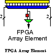
The conventional model results from storing values in registers on
the output of each computational element (See Figures
and
). With this arrangement, we must hold the value on the
output and tie up switches and wires between the producer and the
consumer until such time as the final consumer has used the value. Since
values are produced at different times, and several values from different
sources must converge at a consuming LUT in order for it to produce its
output value, this gives rise to the situation where switches and wires are
forced to sit idle holding values for much longer than the time it takes
for them to transport the values from their sources to their destinations.
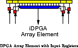
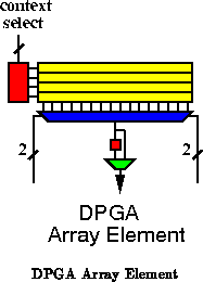
The alternative is to move the value registers to the inputs
of the computational elements (See Figure ). In the simplest
case, this means having four flip-flops on the input of each 4-LUT rather
than one flip-flop on the output. This modification allows us to move the
data from the producer to consumer in the minimum transit time -- a time
independent of when the consumer will actually use the data. We now tie up
space in a register to perform the retiming function rather than tying up
all the wires and interconnect required to route the value from producers
to consumers. Since the register can be much smaller than the intervening
interconnect, this results in a tighter implementation.
Conceptually, the key idea here is that signal transport and retiming are two different functions:
We can view this multicontext progression as successively relaxing the strict interconnect requirements for this class of devices:
A DPGA with input registers (iDPGA) associates an -bit long
shift register with each LUT input in addition to the
instructions per
active LUT. The LUT instruction tells the LUT which of the
values on
the shift register to actually select on each cycle. Each LUT input can
thus retime a value by up to
cycles. That is, values may arrive at the
destination LUT up to
clock cycles before they are consumed.
Figure
shows a possible iDPGA array element with 4
contexts and an input register with depth 3.
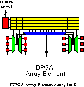
The input registers do place a restriction on the grouping of logical LUTs into physical LUTs which was not present in the original DPGA. Multiple LUTs cannot have inputs arriving at the same input position on the same cycle. Fortunately, LUT input permutability often allows us to rearrange the inputs to avoid such potential conflicts. Nonetheless, the restriction does complicate LUT placement.
The additional resources required for this model are -additional
register cells for each input and one
multiplexor for each
input. For a
-LUT, the area then is:
Composing areas for a 4-LUT, we have:
Note here that we assume the total number of context description bits does not
change. Rather, the bits that indicate which of the inputs to select
are bits which have been shuffled from spatial routing to temporal routing.
That is, this scheme reduces the spatial interconnect requirements by
performing temporal retiming in these registers. We are assuming that the
bits are shuffled from one task to another without any significant change
in the overall number of bits required.
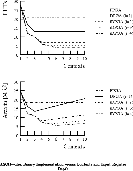
Recall from Section , that our
ASCII
hex binary circuit could be mapped to three contexts, but
could not, viably, be mapped to fewer contexts. By adding the
-input
register as suggested above, the active LUT requirements continue to
decline with throughput reductions. Figure
shows
this same circuit mapped with varying input register depth. As the number
of input registers increases from 1 to 4, the saturation point reduces from
7 active LUTs to 4. Using our area model from the previous section, the
,
iDPGA is 5.5M
, or over 3
smaller than the
single context FPGA implementation at 18.4M
and over 2
smaller than the smallest DPGA without input registers at 12.5M
.
To examine the merits of input registers, we return to our
throughput optimized circuit benchmarks as we originally visited in
Section for DPGAs. We use the same MCNC
circuit benchmark set and the same input netlists as synthesized and mapped
by sis and Chortle. Again, since we are assuming here that the
target criteria is throughput, both sis and Chortle netlists
were synthesized in area mode. As before, no modifications to the mapping
and netlist generation are made.
As before, we divide the multi-context case into separate spatial
pipeline stages such that the path length between pipeline registers is
equal to the acceptable period between results. The LUTs within a phase
are then evaluated in multicontext fashion using the available contexts.
The main difference from Section is
the cost metric for retiming. Since each LUT can retime up to
cycles,
we only charge for retiming registers every
temporal stages between the
original source and the final destination.
When we do need to place retiming registers, they are placed in a
stylized fashion. Starting from the final consumer, we walk back through
the circuit toward the primary inputs, placing a retiming repeater LUT
every th stage. In practice, we often have much more freedom in the
placement of retiming registers, but this freedom was not exploited in our
experimental mapping tools. During the annealing step, whenever the final
consumer for a particular value is moved, the retiming chain is stripped
out and replaced based on the consumer's new location.
After all levelization has been done, a grouping pass is performed.
The grouping pass attempts to group together logical LUTs within a
spatial partition to reside on one physical LUT. For a group of LUTs to be
compatible, it must be possible to permute the LUTs' inputs such that no two
LUTs require a different value to arrive on the same input on the same
clock cycle. Rather than trying all
permutations,
we use a randomized, greedy placement scheme. We randomly pick which input
in a LUT to place first, then greedily place it in a non-conflicting
location. Other inputs within a LUT are placed sequentially after the
initial random selection. The compatibility routine will make several
attempts to find a satisfying assignment before declaring the grouping
incompatible.
Grouping is performed independently on each spatial partition. The grouping routine starts by packing all the logical LUTs in a spatial partition into the minimum number of physical LUTs -- i.e. the number of physical LUTs required to implement the largest temporal stage. The attempt is made by first randomly assigning logical LUTs to physical LUTs, then randomly selecting logical LUTs to swap in order to reduce incompatibility conflicts. Swaps which do not increase the incompatibilities in the grouping are greedily accepted. Swapping continues until a satisfying set of groupings is found or the swapping runs longer than a predetermined time limit which is proportional to the number of logical LUTs which can be described in the spatial partition. When packing fails, we increment the number of target physical LUTs and retry packing.
In review, circuit mapping proceeds through the following steps:
Table shows the total LUTs required after
retiming and packing for the alu2 benchmark mapped to provide a
throughput of one result every four LUT delays. The table shows mappings
for various values of
and
. We constrain
in the current
mapping software, so there are no configurations with
. Up to
,
we see that each additional input register allows us to further reduce the
total number of physical LUTs required in the implementation.
Table
uses the area model from Section
to translate the LUT counts into areas, and Table
shows
the area savings versus a traditional FPGA implementation (
). The
,
, iDPGA implementation is smallest at 43% of the area of the
FPGA implementation.
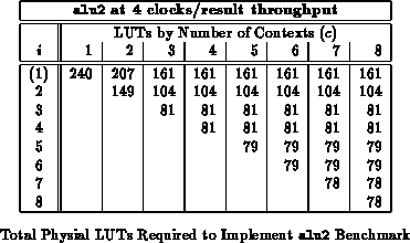
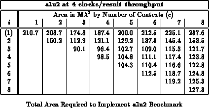
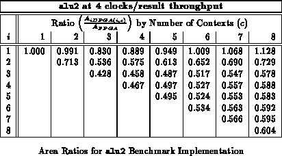
Figure shows the area of the family of
alu2 implementations as a function of context (
) and input (
) depth.
Figure
plots the areas as ratios versus the FPGA
implementation. The first couple of input registers (
goes from
and
) show significant gains for this
benchmark. Gains diminish for greater input register depth. The best
implementations are one-third the size of the FPGA implementation.
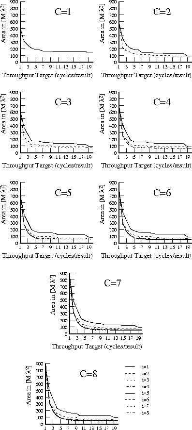
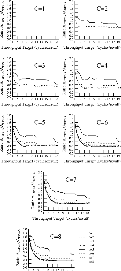
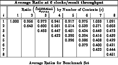
Figure shows the average area ratios across
the entire benchmark set (See Table
)
analogously to Figure
. We see here that an input
register depth of four provides almost all of the benefits of input
registers, with most of the benefit realized by a depth of three, as we saw
with the alu2 case in the previous section.
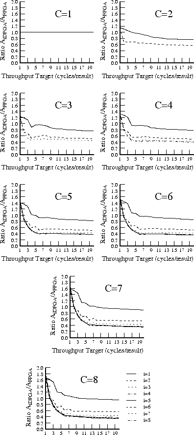
Figure plots area versus throughput for
various context depths (
), at a single values for input depth (
).
Here,
was chosen to give the best results for low throughputs. For
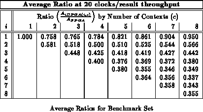
lower throughput values, the 5-8 context cases differ by only 10%.
At the extreme of 20 clocks per result, the
,
case is 33.7% the
size of the single context case, versus the
,
case which is
37.6%.
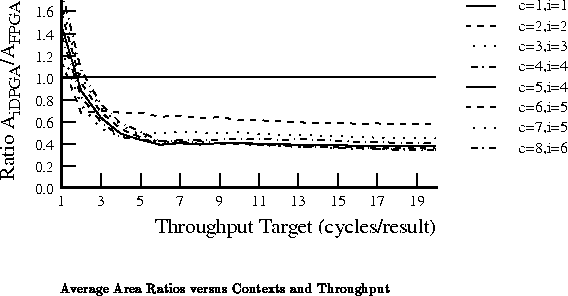
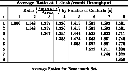
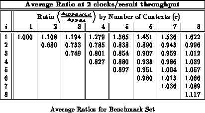
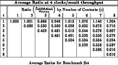
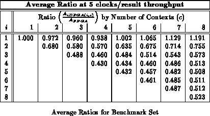
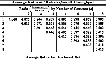
Tables through
record
implementation area ratio for all values of
and
. Each table
reports implemenation areas for a different fixed throughput target in
analog with Table
. For the maximum throughput of one
result per LUT delay, the traditional, single-context FPGA provides the
best implementation. For all other cases, the multicontext implementations
are always smaller than the single-context implementation. With a
LUT-cycle delay in the 7-9.5 ns range, even today's ``high'' throughput
implementations in the 30-50 MHz range are producing new results only once
ever 3-5 LUT delays. At these speeds 3-4 context devices are 40-50%
smaller than the single context implementation. At lower throughputs, the
multiple context implementations are almost one-third the size of the
single-context implementation on average.

As noted previously (Sections
and
), netlist mapping is oblivious of the
final temporal implementations. The allocation of temporal and spatial
pipeline stages is more rigid than strictly necessary. As we noted above
(Section
), retiming LUTs are inserted in a
stylized fashion which is not likely to be optimal. Compatibility
testing is stochastic and may declare many compatible LUT groups
incompatible. Consequently, tighter packing of LUTs is likely with more
sophisticated mapping tools.
Typical tasks require two, different kinds of data transport -- spatial transport to move data from the processing element that generated it to the ones which will consume it and temporal transport to take data from the time when it is generated to the times when it is consumed. It is inefficient to tie up expensive, spatial transport resources such as wires and switches, to perform a temporal transport task. Tasks such as circuit evaluation have sufficient requirements for temporal transport that input retiming registers are clearly a worthwhile architectural feature to include in a multicontext device. Implementations with multiple retiming registers are more compact than implementations with no additional retiming resources.
As with multiple contexts, the extent to which we can save area
with deep input registers depends on the area ratio between the active
interconnect and the retiming registers. Here, we assumed the ratio
between active area and instruction area was 10:1
(800K:78K
), as in the previous chapter. We assumed,
the ratio between the active area and context area including both
instruction and retiming was roughly 8:1 (800K
:104K
).
At these ratios, 4-5 context iDPGA implementations were, on average, half to
one-third the size of the single context alternative.
The best implementation varies with target throughput. At these
size ratios, the ,
case is moderately good across throughput
ranges. It is only worse than the single context implementation at the
highest throughput, and is within 20% of the best implementation at the
lowest throughput measured here.
In the development since Chapter , we have seen that
the area required to implement a general-purpose computational task is
composed of four parts:
For a given computational task, we saw that the requirements for each of these four parts arise from different sources. The number of instructions required to describe the task and number of intermediates held during computation arise from the basic computational task, itself. The size of the active interconnect and processing are dictated by the task's target throughput. For the highest possible throughput, the conventional FPGA strategy of allocating a single instruction to each piece of active interconnect and processing is an efficient allocation of resources. However, as throughput requirements drop below this extreme, multicontext implementations compress the implementation into less space by sharing and reusing a smaller number of active resources. This sharing increases the ratio of instructions and intermediates to active resources. DPGAs are the practical implementation of such a sharing scheme, assigning multiple instructions and multiple intermediate values to each active resource.
Note that the amount of compressibility we achieve with DPGAs is
critically dependent upon how small we can make the non-active residue.
That is, when we remove active interconnect and processing elements, we
are left with the instruction and the intermediate values. The amount of
area savings we can realize depends on how much smaller the space to hold
instructions and intermediates is than the space for the active area
necessary to actually process the instruction and its data. It is this
effect which motivates our interests in reducing the number of bits used to
describe each instruction (Section ) and in reducing the area
required to store those bits ( e.g. DRAM context implementations in
the DPGA prototype -- Section
).
It is also worthwhile to note that the style of compression used in
the last two chapters (Chapters and
), makes
instructions and data readily accessible and is largely independent of task
structure. While densely encoded instructions need some decoding, each
instruction is encoded separately so that it can be stored locally and used
immediately upon being read. If we are willing to pay additional access
latency and work with variable size encodings, block and structure-based
encoding schemes can be used, making it is possible to compress the
instruction requirements further. Ultimately, the minimum task description
area will depend on the descriptive complexity of the task (See
Section
). Exploiting structure, such as, data
widths, operation commonality, and task recurrence requires more general
instruction distribution datapaths and more sequential decoding of task
instructions. Nonetheless, variants on these techniques may be valuable in
further compressing instruction and data residues and hence reducing task
implementation size.