Previous: Time-Switched Field Programmable Gate Arrays Up: New Architectures
Throughout this work, we have seen the central role which
instructions play in general-purpose computing architectures. In
Section , we saw a large architectural space characterized by
the number of distinct control streams, datapath granularities, and
instruction depth. In Chapters
,
,
and
, we reviewed this rich architectural space for
general-purpose computing devices. We saw that the choices made in these
parameters are what distinguish conventional general-purpose architectures,
and we saw that it is these choices that define the circumstances under
which a given general-purpose architecture is most efficient. In
Section
, we saw that even limiting ourselves to datapath
granularity and instruction depth, it is not possible to select a single
pair of these parameters which yielded a robust architecture -- that
is, there is no single selection point whose area requirement will be above
a bounded fraction of the optimal selection of these two parameters for any
task.
Every conventional general-purpose architecture reviewed in
Chapter and summarized in Table
takes
a stand on instruction resources by selecting:
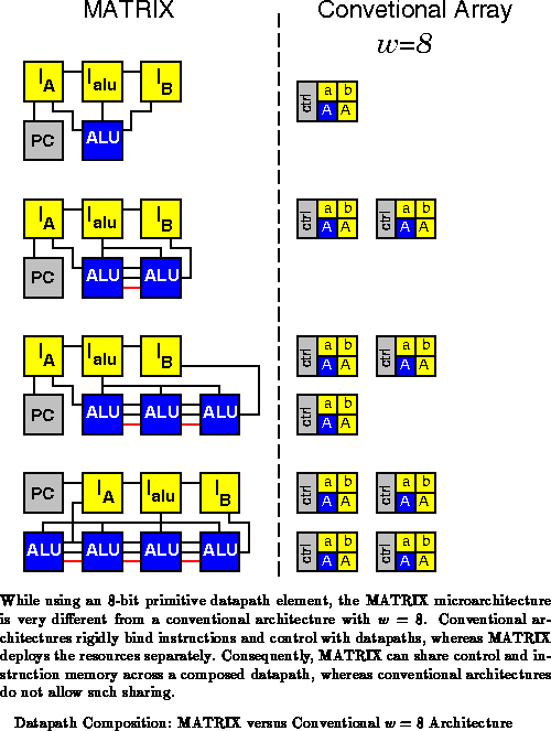
In this chapter, we introduce MATRIX, a novel, general-purpose computing architecture which does not take a pre-fabrication stand on the assignment of space, distribution, and control for instructions. Rather, MATRIX allows the user or application to determine the actual organization and deployment of resources as needed. Post-fabrication the user can allocate instruction stores, instruction distribution, control elements, datapaths, data stores, dedicated and fixed data interconnect, and the interaction between datastreams and instruction streams.
We introduce MATRIX and the concepts behind it. We ground the abstract concepts behind the MATRIX architecture with:
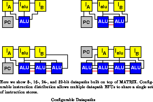
MATRIX is designed to maintain flexibility in instruction control. Primary instruction distribution paths are not defined at fabrication time. Instruction memories are not dedicated to datapath elements. Datapath widths are not fully predetermined. MATRIX neither binds control elements to datapaths nor predetermines elements that can only serve as control elements.
To provide this level of flexibility, MATRIX is based on a uniform array of primitive elements and interconnect which can serve instruction, control, and data functions. A single network is shared by both instruction and data distribution. A single integrated memory and computing element can serve as an instruction store, data store, datapath element, or control element. MATRIX's primitive resources are, therefore, deployable, in that the primitives may be deployed on a per-application basis to serve the role of instruction distribution, instruction control, and datapath elements as appropriate to the application. This allows tasks to have just as much regularity, dynamic control, or dedicated datapaths as needed. Datapaths can be composed efficiently from primitives since instructions are not prededicated to datapath elements, but rather delivered through the uniform interconnection network.
The key to providing this flexibility is a multilevel configuration scheme which allows the device to control the way it will deliver configuration information. To first order, MATRIX uses a two level configuration scheme. Traditional ``instructions'' direct the behavior of datapath and network elements on a cycle-by-cycle basis. Metaconfiguration data configures the device behavior at a more primitive level defining the architectural organization for a computation. Metaconfiguration data can be used to define the traditional architectural characteristics, such as instruction distribution paths, control assignment, and datapath width. The metaconfiguration ``wires up'' configuration elements which do not change from cycle-to-cycle including ``wiring'' instruction sources for elements whose configuration does change from cycle-to-cycle.
In this section we ground the more abstract concepts of the
previous section with a concrete MATRIX microarchitecture. This concrete
microarchitecture will be the focus of the remainder of the chapter. The
concrete microarchitecture is based around an array of identical, 8-bit
primitive datapath elements overlayed with a configurable network. Each
datapath element or functional unit contains a 2568-bit memory, an
8-bit ALU and multiply unit, and reduction control logic including a
20
8 NOR plane. The network is hierarchical, supporting three
levels of interconnect. Functional unit port inputs and non-local network
lines can be statically configured or dynamically switched.
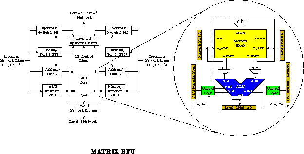
The Basic Functional Unit (BFU) is shown in Figure .
The BFU contains three major components:
MATRIX operation is pipelined at the BFU level with a pipeline register at each BFU input port. A single pipeline stage includes:
The BFU can serve in any of several roles:
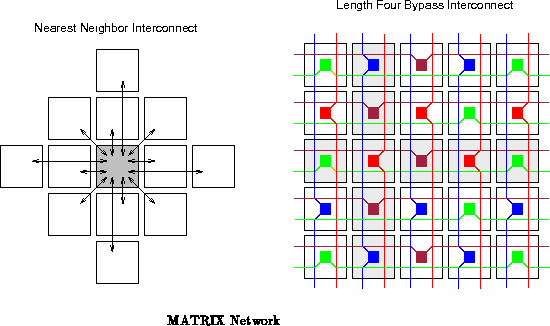
The MATRIX network is a hierarchical collection of 8-bit busses. The interconnect distribution resembles traditional FPGA interconnect. Unlike traditional FPGA interconnect, MATRIX has the option to dynamically switch network connections. The network includes:
Notice that the same network resources deliver instructions, data,
addresses, and control to the BFU ports. All of the eight BFU input ports
(Figure ) are connected to this same network, and all BFU outputs
are routed through this network.
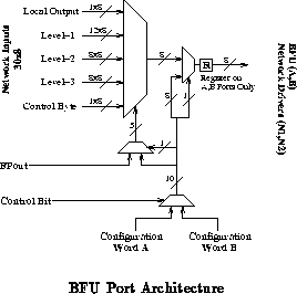
The MATRIX port configuration is one of the keys to the
architecture's flexibility. The input ports are the
primary source of MATRIX's metaconfiguration. Figure
shows the composition of the BFU network and data ports. Each port can be
configured in one of three major modes:
Matrix metaconfiguration information is also multicontext in two ways.
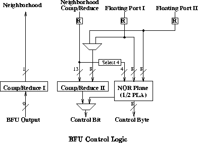
One common use of this control function is in a BFU which operates as the program counter. A typical program counter holds its value ( PC) on the BFU output. In normal operation, the BFU simply increments its current value ( PC=PC+1). When a branch test succeeds, the program counter BFU loads its value from its own memory ( PC=mem[PC]) rather than incrementing. To arrange this, control logic is set to route the ``take branch'' condition on the control bit. One control context is used for the not taken branch case and simply configures the BFU to increment the PC. The other control context is used for the taken branch condition and configures the BFU to use the current PC as an address into memory for a read operation.
Since the control bit can come from the NOR plane, it can be slaved to any bit on any bus distributed to the BFU. This allows a controller to use a BFU or collection of BFUs as two context devices. A single datapath byte can control up to eight such BFUs independently if each BFU is configured to select a distinct bit from the control byte.
The global contexts can also be used to provide DPGA-style multicontext swapping between configurations. Coupling the two programmable contexts with the two control contexts, the entire array can be treated as a four context device without dedicating BFU memory for context data.
The metaconfiguration data for each BFU can be written by
a BFU write operation. The metaconfiguration data is in
a different address space from the BFU local memory. Access to the
metaconfiguration data versus the normal BFU memory is controlled by the
the instruction issued to the BFU memory function port (Figure ).
This arrangement allows the metaconfiguration to be loaded in one of
several ways:
MATRIX ports can also operate in a time-switched mode, inspired by
the time-switched input register (Section ). In
Chapter
, we saw that the ability to latch and hold input
values at designated microcycles, along with switched interconnect, allowed
us to minimize the constraints required during design mapping and thereby
perform physical mapping quickly. Each MATRIX port has a time matching
unit as does memory write back. When metaconfiguration sets a BFU into
time-switched mode, each input is loaded only on its programmed microcycle
as with TSFPGA. The timestep for MATRIX is broadcast along a
designated global line. In time-switching mode, the metaconfiguration
dedicates these global lines and provides for the proper distribution of a
timestep value. Typically, the remaining global lines will be dynamically
switched to provide the necessary interconnect between BFUs. In situations
where light multiplexing is all that is required, the control contexts may
provide sufficient switched routing. For more heavily shared switching
resources, global and bypass lines can be time-switched, with each getting
its own BFU instruction store to control its operation. Time-switched
routing will, of course, slow down MATRIX operation. This mode is
intended primarily for fast, hands-off, automatic mapping during early
development.
The primitives in the architecture do define a granularity at which resources must be deployed. Datapaths and non-local control paths can only come in 8-bit multiples. Context memories come in 256 instruction deep chunks. Compute elements come as 8-bit ALUs with 128-word register files.
Due to the flexible instruction distribution introduced above and
discussed further in Section , MATRIX's granularity does
not have the same kind of effects as conventional architectures
(Chapter
). For task requirements below 8-bits, the datapath
suffers similar to traditional architectures. For task requirements above
8-bits, at most 7-bits of the datapath ever go wasted, and MATRIX does
not waste space on instruction stores holding redundant data as would
conventional 8-bit architectures.
For additional detail on the MATRIX microarchitecture see [Mir96].
In this section we present a range of implementation options for a
single task, convolution, in order to illustrate MATRIX usage and further
ground the features of this architecture. The convolution task is as
follows: Given a set of weights {
,
, ...
} and a
sequence of samples {
,
,
}, compute a sequence of
results
{
,
,
} according to:
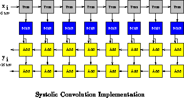
Figure shows an eight-weight (
) convolution of 8-bit
samples accumulating a 16-bit result value. The top row simply carries
sample values through the systolic pipeline. The middle row performs an
8
8 multiply against the constants weights,
's, producing a
16-bit result. The multiply operation is the rate limiter in this task
requiring two cycles to produce each 16-bit result. The lower two rows
accumulate
results. In this case, all datapaths (shown with arrows
in the diagram) are wired using static source mode (Figure
).
The constant weights are configured as static value sources to the
multiplier cells. Add operations are configured for carry chaining to
perform the required 16-bit add operation. For a
-weight filter, this
arrangement requires
cells and produces one result every 2 cycles,
completing, on average,
8
8 multiplies and
16-bit adds per cycle.
In practice, we can:
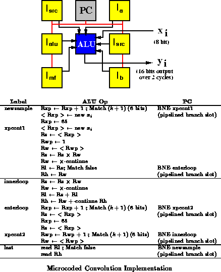
Figure shows a microcoded convolution implementation. The
coefficient weights are stored in the ALU register-file memory in
registers 1 through
and the last
samples are stored in a ring buffer
constructed from registers 65 through
. Six other memory location
(Rs, Rsp, Rw, Rwp, Rl, and Rh) are used to hold values during the
computation. The ALU's A and B ports are set to dynamic
source mode. I-store memories are used to drive the values controlling the
source of the A and B input (two
memories), the values fed into
the A and B inputs (
,
), the memory function (
) and
the ALU function (
). The PC is a BFU setup to increment its
output value or load an address from its associated memory as described in
Section
.
The implementation requires 8 BFUs and produces a new 16-bit result
every cycles. The result is output over two cycles on the ALU's
output bus. The number of weights supported is limited to
by the
space in the ALU's memory. Longer convolutions (larger
) can be
supported by deploying additional memories to hold sample and coefficient
values.
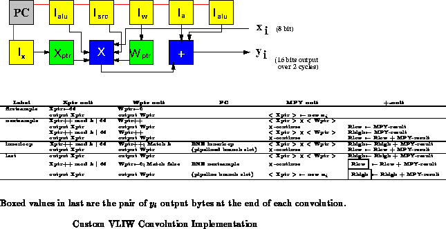
Figure shows a VLIW-style implementation of the convolution
operation that includes application-specific dataflow. The sample pointer
(Xptr) and the coefficient pointer (Wptr) are each given a BFU, and
separate ALUs are used for the multiply operation and the summing add
operation. This configuration allows the inner loop to consist of only two
operations, the two-cycle multiply in parallel with the low and high byte
additions. Pointer increments are also performed in parallel.
Conventional digital signal processors are generally designed to handle
this kind of filtering problem well, and, not coincidentally, the datapath
used here is quite similar to modern DSP architectures. Most of the
I-stores used in this design only contain a couple of distinct
instructions. With clever use of the control PLA and configuration words,
the number of I-stores can be cut in half making this implementation no
more costly than the microcoded implementation.
As shown, the implementation requires 11 BFUs and produces a new
16-bit result every cycles. As in the microcoded example the result
is output over two cycles on the ALU output bus. The number of weights
supported is limited to
by the space in the ALU's memory.
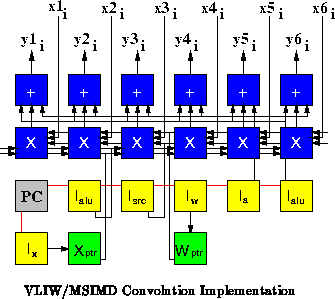
Figure shows a Multiple-SIMD/VLIW hybrid implementation based
on the control structure from the VLIW implementation. As shown in the
figure, six separate convolutions are performed simultaneously sharing the
same VLIW control developed to perform a single convolution, amortizing the
cost of the control overhead. To exploit shared control in this manner,
the sample data streams must receive data at the same rate in lock step.
When sample rates differ, separate control may be required for each different rate. This amounts to replicating the VLIW control section for each data stream. In the extreme of one control unit per data stream, we would have a VLIW/MIMD implementation. Between the two extremes, we have VLIW/MSIMD hybrids with varying numbers of control streams according to the application requirements.
Of course, many variations on these themes are possible. The power of the MATRIX architecture is its ability to deploy resources for control based on application regularity, throughput requirements, and space available. In contrast, traditional microprocessors, VLIW, or SIMD machines fix the assignment of control resources, memory, and datapath flow at fabrication time, while traditional programmable logic does not support the high-speed reuse of functional units to perform different functions.
MATRIX supports flexbile allocation of instruction control
resources as a consequence of the BFU, network, and port architecture
described in Section .
Note that conventional FPGAs are characterized by an instruction depth of one, while an instruction depth of 256-1024 is typical for conventional processor architectures.
Notice also that the ability to assign instruction memories
to composed datapaths is also different from the segmentable
datapaths in modern multimedia processors (Section ),
multigauge SIMD architectures ( e.g. [Sny85]
[BSV +95]), or the Kartashev dynamic architecture
[KK79]. In these architectures, all the
bit processing elements in a predefined datapath perform the same
operation. These generally exhibit SIMD instruction control for the
datapath, but can be dynamically or quasistatically reconfigured to treat the
bit datapath as
,
-bit words, for certain, restricted,
values of
. MATRIX does not have to perform the same ALU function
across all datapath segments like these architectures.
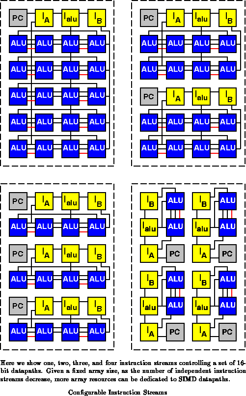
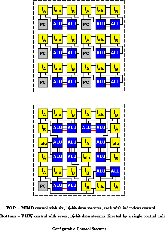
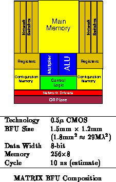
Figure shows the composition of the prototype BFU developed
by Ethan Mirsky [Mir96], along with its size and
projected performance. Table
shows the area breakdown
from the prototype implementation. As described in
Section
, MATRIX operation is pipelined at the BFU level
allowing high speed implementation. With only a small memory read, an ALU
operation, and local network distribution, the basic cycle rate can be
quite small -- at least comparable to microprocessor clock rates. 100 MHz
operation is the target for the prototype design. At 1.8mm
, 100 BFUs
fit on a 17mm
14mm die. A 100 BFU MATRIX device operating at 100MHz
has a peak performance of
8-bit operations per cycle (10 Gop/s).
MATRIX is sufficiently different from conventional architectures
that our model from Chapter does not quite apply. We can
account for the specific composition of our microarchitecture.
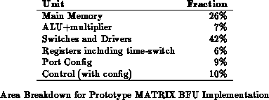
Table
summarizes the constituent elements of the
MATRIX BFU along with estimated areas. The MATRIX size estimate is about
one-third the size of the prototype implementation, suggesting there is
considerable room for improvement relative to the prototype design. The
prototype is a first-generation, one student, university prototype of a
novel architecture. As such, it is not surprising that it is not the most
compact design.
Nevertheless, both area views agree on rough area proportions. Switches and drivers occupy roughly 45% of the area. The main BFU memory accounts for 25% of BFU area. Metaconfiguration makes up roughly 10% of the BFU. The ALU and multiplier composes only 7% of the area.
The MATRIX BFU serves several roles. It is interesting to consider its efficiency in each of these roles.
MATRIX packs 2048 RAM bits into 28.8M in the prototype or,
perhaps, 10M
in an optimized design. If we only use the BFU for
its memory array, each memory bit cell is effectively 14K
, or
5K
, respectively. Of course, the MATRIX memory only comes in
256
8 blocks and will, therefore, be less dense as smaller memories
or memories which are not even multiples of this size are needed.
To get a concrete view of MATRIX application performance, we will examine several image processing primitives implemented in custom and semi-custom silicon and compare them to MATRIX, FPGA, and microprocessor implementations of the same task. LSI's real-time DSP chip set [Rue89] is used to define the tasks and provide the custom implementations. The real-time chip set includes:
LSI's variable shift register takes in byte wide data and delays it
a specified number of clock cycles. It provides eight, equidistant outputs.
The maximum delay supported by the LSI component is clock cycles. That is, given a sequence of inputs:
On the cycle
when
arrives, the VSR outputs eight values:
Here
is a value between 0 and 126. LSI implements their VSR in
64mm
in a 1.5
CMOS process (114M
) using a semicustom
standard cell methodology. The LSI VSR runs at a 26 MHz clock rate (38.5ns
clock).
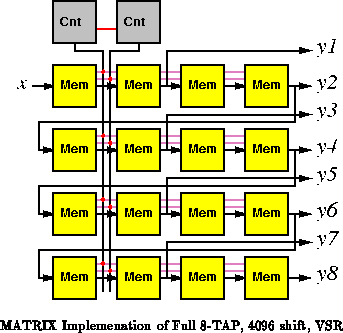
A MATRIX implementation providing the full, worst-case
functionality of the VSR requires two BFUs to implement each 512 byte tap
and two BFUs to implement a 9-bit modulo counter, for a total of 18 BFUs
(See Figure ).
The memory BFUs implement the shift register by alternately reading and
writing from their main memory. The control contexts are programmed to
support the two instructions, read and write. The counter counts on every
cycle from zero to
. The low bit of the
counter is selected as the control bit on the memories while the high 8
bits serve as the memory address. The match unit on the counter is set to
look for
. When a match occurs, the counter executes a load
zero control context instead of the normal increment context. The 18 BFUs
take 28.8M
. Operating on the
two clock macrocycle, the MATRIX VSR can run at 50MHz (20ns macroclock).
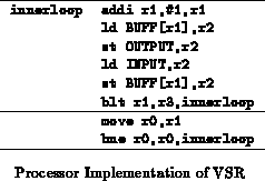
A typical processor implemenation of VSR (See Figure )
takes 6 instructions per tap in a tight loop. For the full 8 tap VSR, the
processor implementation requires 48 instructions. MIPS-X
[HHC +87], one of the highest capacity processors we reviewed in
Table
, is 68M
. With a 50ns clock
cycle, the 48 instructions will dictate, at least, a 2400ns macroclock.
An FPGA implementation would be dominated by data memory. A pure
4-LUT design would require up to 40968=32K cells. At
600K
, a low-end estimate for 4-LUT size (See
Table
), this is 19.7G
.
Exploiting the memory in an XC4000 part, we can pack 16
2 bits per
CLB, requiring 256
4=1K CLBs or 1.28G
. The full shift
register approach is trivial and
should be very fast, so we will assume 100MHz operation. Exploiting the
XC4000 memories will require both a read and a write operation as with
MATRIX so we will assume it can achieve 50MHz operation.
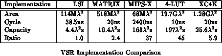
Table compares the VSR implementations. The
MATRIX implementation is 2.4
larger than the semicustom LSI
implementation, 2.5
smaller than the XC4000 implementation, and
16
smaller than the processor implementation. If the shift
register requires less than 2048 delay slots, MATRIX can implement each tap
with a single BFU and use a single counter. This cuts the implementation area
and capacity in half, bringing it within 20% of the capacity of the LSI
implementation. Smaller shift registers with fewer taps will allow further
reduction in BFUs for the MATRIX implementation. Capacity requirements for
the FPGA implementations similarly reduce with total shift register length.
The capacity required for the processor implementation will decrease with the
number of taps.
LSI's rank value filter selects the th largest 12-bit value within
a 64 sample window. That is, on each cycle, the component takes in a new
12-bit sample,
. It looks at the previous 64 values (
,
, ...,
), and selects the
th largest, which it
outputs as
. If
, it implements a maximum filter; if
, it
implements a minimum filter, and if
, it implements a median filter.
The LSI implementation occupies 132mm
in a 1.5
CMOS process
(235M
) using an array design methodology. The RVF runs at a
27 MHz clock rate (37ns clock).
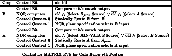
The MATRIX implementation of RVF maintains a completely ordered list of the 64 window values using a systolic priority queue scheme similar to [Lei79]. The systolic priority queue allows it to compute incremental updates to the list ordering rather than recalculating the entire ordering on each cycle. To simulate the 64 tap window scheme, the systolic queue supports both an insert and a delete operation. Each macrocycle requires two microcycles -- one in which the old value is deleted and one in which the new value is inserted. A fixed delay register scheme like the VSR is used to retime the old value for deletion 64 macrocycles later.
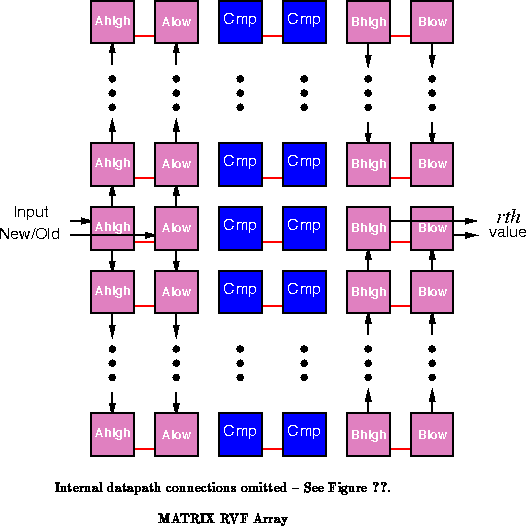
Using this style, an -tap,
-bit wide MATRIX RVF implementation
requires
BFUs, or 386 BFUs for the
64 tap, 12-bit case as implemented in the LSI filter. Each tap requires
two active data swap registers (
and
) and a comparator, each of
which needs to be as wide as the sample data.
Figure
shows the basic array structure for the
12-bit sample case where two BFUs are required for each register and
comparator. The additional two BFUs are used for the retiming memory and
its associated counter. Figure
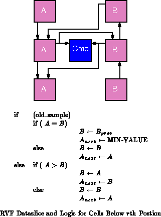
shows details of
the datapath for a tap slice and its adjacent elements. The
registers
are used to propagate insert and delete values while the
registers are
used to hold sorted values.
values propagate away from the
th item
and
values propagate toward it. By inserting data at the
th value
location, we obtain an update latency of only one macrocycle or two
primitive MATRIX cycles. The logic for a datapath slice is described in
Figure
. Note that the logic and datapath shown
are for a tap position below the
th position in the array. The logic
and flow are reversed for tap positions above the array.
Figure
shows the control setup used to implement the
datapath logic providing single cycle throughput for each comparison and
swap operation.
We use a similar insert and delete structure for the processor RVF
implementation which is shown in Figure . For any width less
than the processor word size, the processor implementation requires
instructions in a tight loop. For the full 64 tap VSR, the processor
implementation requires 649 instructions. Again, using the MIPS-X processor
this requires 68M
and
.
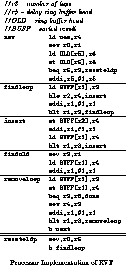
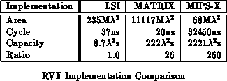
Table compares the RVF implementations. The
MATRIX implementation is 26
larger than the custom implementation
and 10
smaller than the processor implementation. If less taps are
required, both the matrix and the processor implementation decrease
linearly in the number of taps. For 8-bit or smaller sample values, the
MATRIX implementation will halve its datapath requirements. If one only
wants to filter for the maximum or minimum value, a straightforward shift
and compare reduce scheme will only require
BFUs and operate at
100MHz throughput. For a maximum or minimum filter, the MATRIX
implementation requires less capacity than the LSI RVF for 8-bit filters
with less than 16 taps or 12-bit filters with less than 8 taps.
LSI's binary filter and template matcher performs binary template matching across a 1024 bit template. That is:
Here is a vector of 1024 bit match values and
is a mask indicating
which positions are ``don't care'' values and should be ignored. LSI
implements their VSR in 88mm
in a 1.5
CMOS process
(156M
) using a full custom design methodology. The LSI BFIR
runs at a 27 MHz clock rate (37ns clock).
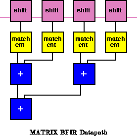
The MATRIX implementation comes in three parts shown in
Figure . A set of shift registers provide the bit level
samples. A set of BFUs use their memories to perform matching and
counting, starting with 8 bits of input and producing a 4-bit sum of the
number of matches. Finally, an adder tree reduces the partial sums to a
single result. To handle the 1024 tap problem, MATRIX requires
BFUs for bitwise shifting and another 128 BFUs for
matching. The sum tree is 7 stages deep. Since the final two stages add 9-
and 10-bit sums, they each require 2 BFUs per addition, while each of the
others requires a single BFU per sum, making for a total of 130 BFUs in the
adder tree. Together, the MATRIX implementation requires 386 BFUs
(11.1G
) and can operate at the full 100MHz basic cycle rate.
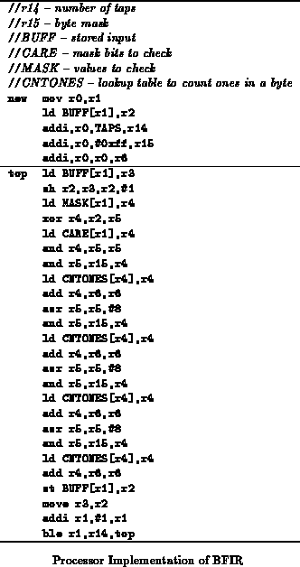
The processor implementation shown in Figure stores
and masks data in 32-bit units to exploit its datapath. It also uses a
programmed lookup table to count ones. The processor only counts ones a
byte at a time so that the count one's lookup table can fit in a reasonably
sized data cache. The main loop takes 25 instructions per word. For a
1024 tap problem, this makes
total instructions. The MIPS-X processor implementation
then is 68M
and
.
An FPGA BFIR could take a similar form to the MATRIX
implementation. 1024 LUTs would compose the shift register.
4-LUTs compose the match
and initial reduce. The sum tree requires slightly over 1000 full adder
bits -- 1000 XC4K CLBs or 2000 4-LUTs. In total, an XC4K implementation
would require 1850+ CLBs, or 2.3G
. Using the fast carry on the
XC4K, and pipelining the adder stages, the basic cycle could be as low as
10ns assuming an optimal physical layout.
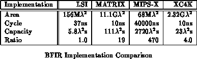
Table compares the BFIR implementations. The
MATRIX implementation is 19
larger than the custom implementation,
4.8
larger than the Xilinx implementation, and 24
smaller
than the MIPS-X implementation. If the ``care'' region is sparse, the FPGA
implementation can easily take advantage of it, using less match and sum
reduce units ( e.g. [VSCZ96]). If the sparsity is in
8-bit chunks, MATRIX can similar exploit the sparseness. The processor
implementation can exploit sparseness, as well, but requires even larger
chunks for it to be beneficial. Resource requirements for all the
programmable implementations are proportional to the template size, so their areas decrease with the number of binary taps.
The LSI multibit finite-impulse response filter is a 64-tap, 8-bit
FIR filter:
The MFIR is implements in 225mm
in a 1.5
CMOS process
(400M
) using a full custom design methodology. The LSI MFIR
runs at a 22 MHz clock rate (45ns clock).
In Section , we have already seen several MATRIX
FIR implementations. To handle the same generality as the LSI MFIR, we
need to handle a 24-bit accumulate instead of the 16-bit accumulate used in
the examples shown in Section
. This adds one cycle per
tap to the microcoded implementation, one BFU to the VLIW implementation,
and one BFU per tap to the systolic implementation. Table
compares the LSI and MATRIX implementations along with processor and DSP
implementations. For the table, we use an application-specific metric and
report the area-time capacity required per TAP in each of the
implementations.
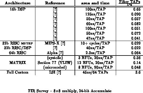
The systolic MATRIX implementation is 6 larger than the full-custom
LSI implementation, 20
smaller than the MIPS-X processor
implementation, and 9
smaller than the Alpha implementation.
Note also that the VLIW MATRIX implementation, which resembles modern DSP
architectures, is 2
smaller than modern DSPs. The systolic version
is 8
smaller than the DSPs. The capacity requirements for the
processors, DSPs, and MATRIX will decrease with the number of taps, while
the LSI implementation is fixed. At 10 filter taps, the systolic MATRIX
implementation uses less capacity than the LSI MFIR.
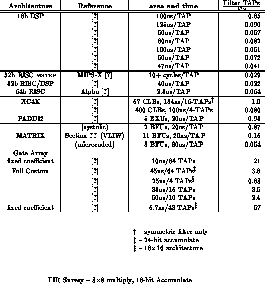
Table provides an expanded table for FIRs with 16-bit
accumulates. Here, we see more clearly that the systolic MATRIX
implementation is on par with reconfigurable implementations such as PADDI
and FPGAs. The MATRIX VLIW is comparable to DSPs. The MATRIX microcoded
yields performance comparable to microprocessor implementations. It is
this versatility to efficiently span such a wide range of raw performance
requirements which makes MATRIX an interesting and powerful general-purpose
architecture.
Across the four tasks, we see that the MATRIX implementation is
roughly an order of magnitude larger than the custom implementation
(6, 19
, 26
, and 2.4
). Since it remains
general-purpose, MATRIX retains the ability to deploy resources to adapt to
the problem size. For many instances of problems the area-time penalty
will be much less.
At the same time, we saw that MATRIX provided an order of magnitude
smaller implementations than conventional processors
(16,10
,24
,20
). The variation in the
benefits is somewhat telling. The one task where MATRIX only had a
10
advantage is the one task which required a 16-bit datapath,
while all the others essentially used 8-bit datapaths. Combining that
observations with our earlier observation that MATRIX has 3
the raw
computational density of modern processors, we can decompose MATRIX's
capacity advantage over processors as:
roughly as:
For the highest throughput implementations of these tasks,
aggressive FPGA or DPGA implementations may approach the MATRIX
implementation. We saw cases where MATRIX was 2-10 smaller than
optimistic FPGA implementations. We also saw naturally bit-level tasks
where MATRIX might be 4-5
worse than an FPGA implementation.
All conventional, general-purpose computing architectures set the resources for instruction distribution and control and bind datapaths to instructions at fabrication time. This, in turn, defines the efficiency of the architecture at handling tasks with a given wordsize, throughput, and control structure. Large applications typically work with data items of multiple sizes and subtasks with varying amounts of regularity. Application sets have an even wider range of computational task characteristics. Consequently, no single, fixed, general-purpose architectural point can provide robust performance across the wide range of application requirements.
To efficiently handle the wide range of application characteristics seen in general-purpose computing, we developed MATRIX, a novel general-purpose architecture which uses multilevel configuration and a single pool of network and datapath elements to defer until application run time:
An ongoing prototyping effort shows promising results. While the
VLSI implementation has considerable room for improvement, the prototype
has 3 the raw computational density of conventional processors and
achieves 10
the yielded computational density on regular,
byte-level computing tasks. At the same time, the prototype holds its own
on less regular tasks, achieving performance comparable to conventional
processors.
The concrete microarchitecture presented here has been our initial vehicle for studying the basic concepts behind MATRIX and providing a concrete grounding for them. In these respects the concrete microarchitecture has been very successful. However, this microarchitecture fails to achieve the full breadth of performance robustness promised by the MATRIX architectural style.
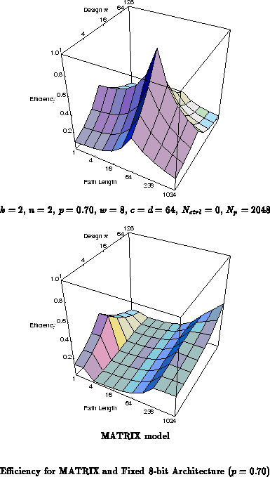
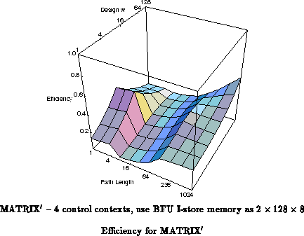
Figure shows the efficiency of the MATRIX
microarchitecture at handling tasks with various instruction depths and
datapaths widths. Shown alongside MATRIX is the efficiency for a
conventional architecture with fixed instruction distribution. These
graphs are similar to the one shown in Section
. The
efficiency is the ratio between the size of the implementation in the
target architecture versus the size of the conventional architecture with
the instruction depth and datapath width perfectly matched to the task.
We assume here that MATRIX must deploy eight BFU instruction stores
per independent datapath for control. That is, we assume all eight MATRIX
ports must be fed with dynamic instructions.
It is not surprising that MATRIX does not have the peak performance of the fixed architecture at its optimal design point. However, the poor efficiency across such a broad range of space is disappointing. We can identify several effects from the graph:
Also shown in Figure is a MATRIX
architecture which lessens the BFU overhead penalty for cases with a path
length between 2 and 256. MATRIX
assumes that it can use each
BFU memory as two 128
8 instruction stores, bringing both memory
read ports out to routed lines and allowing path lengths less than
to use only four BFUs per datapath. MATRIX
also assumes the
addition of two more control contexts.
These graphs suggest: