

 Previous: Review and Extrapolation Up: Review and Extrapolation Next: Projections
Reconfigurable Processing Architecture Review

Special-Purpose Computing
We build computing devices to algorithmically transform raw input
data into results. Special-purpose computing devices are designed with one
particular transformation embedded into their architecture and
implementation. Each such device can solve only the particular
transformation problem, and that problem is set prior to device
fabrication. Conventional fabrication techniques require long turn-around
(weeks to months) to produce devices, high up front costs for setup, and
large volume sales to amortize out fixed costs for design, tooling, and
equipment.
Many of the characteristics which come with special-purpose
computing devices are undesirable or untenable in numerous situations.
- Device dedicated to a single function
- Device can be quickly oboslesced as
functional requirements often change, transformations
are tuned, algorithms advance, and missions and tasks evolve.
- When the function needed by a task is time or data dependent
the special-purpose devices for functions which are not needed
at some point in time sit idle and cannot be used for any
other function which may be required by the task.
- When lower throughput is required from the device than
its native capability, the device has spare capacity which
cannot be put to productive use.
- High up front cost
- Long delay from concept to delivery
- Economical only in volume
General-Purpose Computing
General-purpose devices are our alternative to these fixed function
devices. Here, we build computing devices
which can be configured to solve
a variety of computing problems. Instead of building a device with exactly
the computational units and hardwired dataflow necessary to solve a single
problem, we build a device with a set of primitive computational elements
interconnected via a flexible interconnect. Post-fabrication, we control
the behavior of the device with instructions, extra inputs which tell the
device what computations to perform and how to route data during the
computation. As a result, we:
- Make a single device appealing for a wide-range of tasks.
While each, individual task may lack the volume required
for a dedicated device to be economical, the general applicability
across many tasks provides the volume necessary to make the
general-purpose device economical.
- Eliminate the fabrication delay necessary to put a new
computational task into use.
- Eliminate the up front cost associated with producing custom
hardware for a task.
- Make it possible to customize a single device to perform any of a
large number of different computing task, allowing the device to adapt
to changes in requirements, or share its capacity among a variety of
computing tasks.
The RP-space defined here models a large domain of reconfigurable
architectures within the general-purpose architecture space.
Reconfigurable Computing Costs
Reconfigurable devices gain their breadth of use at a cost in
computational density. Reconfigurable devices must add:
- Flexible interconnect or data flow
- Instructions to control compute units and data flow
Additionally, the computational units in these devices must be
more general than in the special-purpose devices where each compute
unit may perform a single, focussed computation.
Replacing fixed interconnect with flexible interconnect is the most
costly single addition for reconfigurable architectures. A decent amount
of programmable interconnect may add two orders of magnitude in size to the
reconfigurable implementation compared to the fully special-purpose
implementation of the same task.
Instructions
In contrast, the area required to hold a single, device-wide
configuration is, itself, an order of magnitude smaller than the
interconnect. That is, the area taken by a single instruction is generally
an order of magnitude smaller than the active interconnect which it
controls. However, if we allocate space to hold tens of instructions per
active compute element, the total instruction memory area can easily equal
the active compute and interconnect area. By the time we add hundreds of
instructions, the instruction memory area can dominate even the flexible
interconnect. With this additional order of magnitude in overhead, such a
reconfigurable device can easily be three orders of magnitude larger per
computational element than its special-purpose counterpart.
Since instruction area can quickly come to dominate even the
flexible interconnect, when building reconfigurable computing architectures
we often look for structure in typical computational problems which will
allow us to reduce the instruction size. One common technique is to
control several pieces of interconnect and computational elements with a
single instruction. That is, we assemble wide datapaths which are
controlled together. This reduces the size of the configuration by
reducing the number of instructions required to specify device behavior at
any point in time.
Consequently, when we build a reconfigurable computing device, we
must make decisions about:
- How many primitive computational elements are directed by
each instructions?
- How many instructions are controlled by each controller?
- How many instructions are stored on chip?
- How rapidly can the instructions change, chip-wide?
The answers to these questions place a particular reconfigurable device in
the RP-space. The answers to each of these questions also determines
the size of the reconfigurable device and its efficiency on various tasks.
- If the task has data elements of width of
 ,
the architecture provides finer instruction control than
necessary and pays an overhead for redundant instruction memory.
,
the architecture provides finer instruction control than
necessary and pays an overhead for redundant instruction memory.
- If the task has data elements of width of
 ,
the architecture does not allow control over the compute
element at the fine granularity of the task, and
computational capacity in the architecture goes to waste.
,
the architecture does not allow control over the compute
element at the fine granularity of the task, and
computational capacity in the architecture goes to waste.
- If the task needs to cycle through only a few different
instructions, but the architecture provides large instruction
memories, the reconfigurable device is unnecessarily large
for the task, wasting area in unused memories.
- If the task needs to cycle through a large number of different
instructions at different times but the architecture
provides small instruction memories, the reconfigurable
device will not be able to store all the instructions
logically associated with each computational element.
Extra computational elements will be required simply
to hold all of the task's instructions, but these extra
computational elements will effectively sit idle during
computation.
- If the task requires more independent control of computing
resources than provided by the architecture, either resources
will go unused since they cannot be controlled or memory
requirements will increase greatly to compensate for the
lack of control independence.
- If the task requires less independent control than
the architecture supplies, the additional controllers and
resources are redundant and add to device overhead.
- If the task requires rapidly changing instructions, but the
architecture does not meet the required bandwidth,
computational resources sit idle, paced by task description
bandwidth not the availability of computing resources.
- If the task can handle slowly changing instructions, but the
architecture dedicates significant area to providing high
instruction delivery bandwidth, much of the dedicated area is
overhead making the device larger than necessary for the task.
Interconnect
In devices where the ratio between instructions and compute
elements is low, flexible interconnect will remain the dominant area
feature in reconfigurable devices. Here, a device must decide how richly
to interconnect the compute elements. Rich interconnect makes the
routing area even greater, while inadequate interconnect can make it
impossible to make use of the available computing elements. The choice
in interconnect richness determines where the architecture will be most
efficient.
- If the interconnect is richer than needed by the task, the
device will be larger than necessary.
- If the interconnect is not as rich as required by the task, the
task must be laid out sparsely on the architecture. Portions of
the interconnect and compute resources are wasted as they cannot be
used.
In all computing devices there are two components associated
with routing data between producers and consumers:
- Spatially routing intermediates from the compute element which
produced them to those which consume them
- Retiming the intermediates for the time when the consumer is ready
to use them
Particularly, in reconfigurable devices with expensive, flexible
interconnect, memories can hold values for retiming more cheaply than
active interconnect.
Degrees of Generality and Reconfigurability
There are, of course, degrees of ``generality'' between fully
special-purpose devices and general-purpose devices. Some special-purpose
devices are given limited configurability to broaden there use --
e.g. a typical UART can be configured to handle different data sizes, data
rates, and parities. Some devices are targeted at being ``general'' within
very specific domains. Digital signal processors are one of our most
familiar examples of a general-purpose, domain-optimized device. The
domain may dictate the typical data element size or desirable instruction
depth. Further, the domain may allow a more structured programmable
interconnect to suffice. Nonetheless, to the extent that we have
post-fabrication control over the computations which a device performs, the
device will have some form of instructions and will generally have some
level of flexible interconnect. With these features it exhibits
reconfigurable characteristics, and many of the the architectural
characteristics, relations, and issues we have identified in our, more
ideal, RP-space.
FPGAs
Conventional FPGAs fall at a moderately extreme point in
our RP-space with single bit wide datapaths and single instruction
deep instruction memories. At this point, they are efficient on the
highest throughput, fine-grained computing tasks and their efficiency drops
rapidly as the task throughput requirements diminishes and the word size
increases.
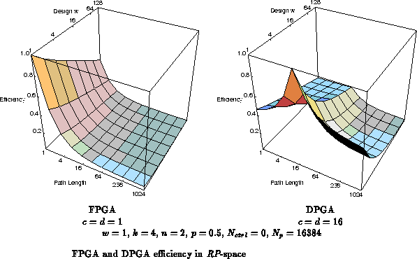
Beyond FPGAs in the Reconfigurable Computing Space
Beyond FPGAs there is a rich reconfigurable architecture space.
Our DPGA represents one different point in this architectural space (See
Figure  ). The DPGA retains the bit-level
granularity of FPGAs, but instead of holding a single instruction per
active array element, the DPGA stores several instructions per array
element. The memory necessary to hold each instruction, is small compared
to the area comprising the array element and interconnect which the
instruction controls. Consequently, adding a small number of on-chip
instructions does not substantially increase die size or decrease
computational density. The addition does, however, substantially increase
the device's ability to efficiently handle lower throughput, more irregular
computational tasks. At the same time, a large number of on-chip
instructions is not as clearly beneficial. While the instructions are
small, their size is not trivial -- supporting a large number of
instructions per array element ( e.g. tens to hundreds) would cause a
substantial increase in die area decreasing the device efficiency on
regular tasks. Consequently, we see that we can achieve a design point
which is moderately robust across a wide range of throughput variations by
balancing the instruction memory area with the fixed area for interconnect
and computational units.
). The DPGA retains the bit-level
granularity of FPGAs, but instead of holding a single instruction per
active array element, the DPGA stores several instructions per array
element. The memory necessary to hold each instruction, is small compared
to the area comprising the array element and interconnect which the
instruction controls. Consequently, adding a small number of on-chip
instructions does not substantially increase die size or decrease
computational density. The addition does, however, substantially increase
the device's ability to efficiently handle lower throughput, more irregular
computational tasks. At the same time, a large number of on-chip
instructions is not as clearly beneficial. While the instructions are
small, their size is not trivial -- supporting a large number of
instructions per array element ( e.g. tens to hundreds) would cause a
substantial increase in die area decreasing the device efficiency on
regular tasks. Consequently, we see that we can achieve a design point
which is moderately robust across a wide range of throughput variations by
balancing the instruction memory area with the fixed area for interconnect
and computational units.
The importance of efficiently supporting retiming of intermediates
was most clearly demonstrated in the context of the DPGA design. Here, we
saw that the benefits of deeper instruction memories were substantially
reduced if we forced retiming to occur on active interconnect. However,
when we provided architectural registers so that retiming could take place
in registers, DPGAs were able to realize typical computing tasks in one-third
the area required by conventional FPGAs.
While we did not detail them in this thesis, multiple context components
with moderate datapaths also come down essentially in this reconfigurable
architectural space. Pilkington's VDSP [Cla95] has an 8-bit
datapath and space for four instruction per datapath element. UC
Berkeley's PADDI [CR92] and PADDI-II [YR95] have a
16-bit datapath and eight instruction per datapath element. All of these
architectures were originally developed for signal processing applications
and can handle semi-regular tasks on small datapaths very efficiently.
Here, too, the instructions are small compared to the active datapath
computing elements so including 4-8 instructions per datapath substantially
increases device efficiency on irregular applications
and robustness to throughput variations with minimal impact on die area.
Flexible Deployment of Instruction Resources
While architectures such as these are often superior to the conventional
extremes of FPGAs, any architecture with a fixed datapath width, on-chip
instruction depth, and instruction distribution area will always be less
efficient than the architecture whose datapath width, local instruction
depth, and instruction distribution bandwidth exactly matches the needs of
a particular application. Unfortunately, since the space of allocations is
large and the requirements change from application to application, it will
never make sense to produce every such architecture and, even if we did, a
single system would have to choose one of them. Flexible, post
fabrication, assembly of datapaths and assignment of routing channels and
memories to instruction distribution enables a single component to deploy
its resources efficiently, allowing the device to realize the architecture
best suited for each application. Our MATRIX design represents the first
architecture to provide this kind of flexible instruction distribution and
deployable resources. Using an array of 8-bit ALU and register-file
building blocks interconnected via a byte-wide network, our focus MATRIX
design point has 3 the raw computational density of processors and
can yield 10 the computational density of conventional processors
on high throughput tasks.
the raw computational density of processors and
can yield 10 the computational density of conventional processors
on high throughput tasks.