Previous: Reconfigurable Processing Architecture Review Up: Review and Extrapolation Next: Review of Major Concepts
In Parts and
, and
Chapter
, we focussed on reconfigurable, general-purpose
computing devices roughly characterized by RP-space. In that focussed
domain, we were able to look closely at area costs, computational density,
and efficiencies. General-purpose devices, more broadly, also share many
of the characteristics ( e.g. instruction depth and width, interconnect
richness, data retiming) which we identified as key architectural
parameters in RP-space and in the more detailed architectural
studies. In this chapter, we speculate more broadly on what the
relationships developed while focusing on reconfigurable devices in
RP-space might tell us about general-purpose architectures, in general.
We emphasize that these extrapolations may overly trivialize important
architectural aspects which did not arise in RP-space, and we attempt
to identify those aspects during the discussion.
In our computing architectures, we have seen memory show up in two roles:
Instruction memories reduce hardware requirements in two ways by allowing:
We can return to our pedagogical 4-LUTs to see this reduction more
concretely. There are
different functions which can be implemented with
, four-input gates.
So, even with the 100
area overhead per gate required to
support flexible interconnect, our programmable,
4-LUT device is
significantly smaller than implementing all possible
input functions
for anything other than trivial values of
.
What we trade for this reduction is computational throughput. With
only active computing functions, it requires us, at least,
cycles to perform the computation of the
primitive
computing functions in the original task. Sometimes, the original task
already had a dependency structure such that this reduction comes
for free or at minor costs. Other times, we are trading increased
evaluation time for reduced implementation area. In the limit, where we
have a single computing element with instruction memory to hold
instructions, the task can take
cycles to evaluate.
We often talk about virtualizing hardware resources. The virtualization really substitutes a less expensive resources ( e.g. an instruction in memory, state in memory, cheaper forms of memory) for a more expensive one ( e.g. a piece of hardware to actually perform a function, fast access memory). Behind all of these virtualizations, we must ultimately have some form of physical memory to hold the description of the virtualized resources and their state.
Notice that we can continue to push technology and structure in order to reduce this last limit, but it cannot be avoided. We can apply aggressive memory technology, such as DRAM or flash memory, to reducing storage cell size. We can store data on different media, such as magnetic disks or tape. We can exploit structure in the task description to compress the number of bits required down to the Kolmogorov complexity limit. In the limit, however, we ultimately require sufficient area to store the description of the computing task and no further reduction is possible.
We noted in Section that memory can be used as a
general-purpose computing element. That role of memory is a special case
of role of memory as instructions. The memory contents act as an
instruction which configures the memory array to provide the desired
computational transformation between the address inputs and the data
outputs. In Section
, we saw that computational portion of
conventional FPGAs, the LUTs, were programmed in exactly this way.
Once we begin to reuse primitive compute functions for different roles at different times, we introduce the need to assure that the right data arrives at the inputs of the function at the right time. This need is particularly acute when we serialize execution and use a single primitive to perform multiple different functions, but it also appears when we reuse a primitive to perform exactly the same function on logically different data. Since programmable interconnect is expensive, we use memories as an inexpensive way to provide the temporal retiming necessary for correct execution.
The use of memory for retiming is pragmatic. We could get away with little more than pipeline registers on interconnect. However, it is cheaper to transport data forward in time through memory than over interconnect. If we do not take advantage of this, much of the area savings potentially associated with serializing execution and sharing primitive compute elements cannot be realized.
The requirements for data retiming depend on the interconnect structure of the problem, not the number of compute elements in the task. The amount of retiming does depend on the amount of serialization. With more parallelism, more data can be consumed as soon as it has been spatially routed avoiding the need for retiming. As we compress size requirements by converting task compute primitives into instructions sharing a small number of physical compute elements, we must ultimately have space to store all computation intermediates at the widest point in the computation flow. That is, we ultimately need space for all the live intermediates in a computation. The number of such intermediates depends on the task and its mapping. The mapping should try to minimize the number of such intermediates.
Note that all non-instruction uses of memory fall into this category.
Even special-purpose devices often sequentialize their processing of data so that a few, fixed compute elements can serve to process data with nominally different roles. The most common example of this is in audio, video, or image processing. Rather than dedicating a separate computational unit to each pixel in a frame, many pixels are processed on the same computational unit. The pixel data stream is serialized into and out of the special-purpose device. The pixels within the frame often need to be retimed so that the right pixel values are presented to the compute elements at the right time. For example, when pixels are fed in by rows, it is often necessary to perform row-wise retiming on data so that the compute element can calculate column-wise interactions between pixel elements. If all the data necessary for the computation were presented simultaneously and all of the output was produced at once, this retiming would not be necessary. However, serialization and reuse is often necessary to make the amount of hardware resources, including component input and output bandwidth, tractable. The serialization allows us to share all of the hardware resources, but requires that we provide unique storage space for intermediate data so that we perform the correct computation on the shared resources.
There are two important ideas to take away from these observations on the role of memory:
Device architects are often faced with the dilemma of balancing semantic expressiveness with instruction distribution bandwidth. In processors, only a few bits are allocated to instruction specification limiting (1) the number of different computations which can be selected and (2) the number of different sources which can be expressed. The latter manifests itself as limited address space and limited size register files, while the earlier is often taken for granted. Architects are reluctant to increase instruction width because it entails added costs in (1) on- and off-chip storage space for all instructions, (2) distribution bandwidth, and (3) power for instruction distribution. However, limited semantic expressiveness can force the processor to issue a large number of instructions to perform the desired computation, resulting in even great losses in time and power efficiency.
Conventional processors generally support an ALU which performs basic operations on 2 or 3, word-wide data inputs. Today we see typical word sizes of 32 and 64 bits. Conventional processors further limit their instruction size to the word size to limit instruction bandwidth requirements. As a consequence of this limitation, it can often take a large number of instructions to specify an operation which is not inherently difficult for the active silicon to perform.
To appreciate the magnitude of the semantic disparity here, we notice that
there are:
functions from two
-bit wide inputs to one
-bit wide output. If we
limit the specification of our function to
bits, we can only address
functions with this instruction. Thus, if all of the
were equally likely, on average, it would take at least
cycles to compute a function.
In practice, a good fraction of the bits are dedicated to operand
selection, increasing the severity of the instruction limitation. While
all operations are not equally likely, in practice, this disparity
demonstrates that conventional processor design makes an early
binding, pre-fabrication time, decision on the effective cost of basic
operations. Many applications cannot use the active silicon area
on conventional processors efficiently since they cannot directly issue the
instructions native to the task.
Reconfiguration is a technique which allows us to find a resolution
to this dilemma. Reconfiguration allows us the semantic expressiveness of
very large instructions without paying commensurate bandwidth and deep
storage costs for these powerful instructions. What we give up in this
solution is the ability to change the entire instruction on every cycle.
Rather, the rate of change of the full instruction is determined by the
instruction bandwidth we are willing to expend. The distinction between
instruction bandwidth which delivers all the semantic content on every
cycle and instruction bandwidth that can be used to load a larger semantic
instruction is an important one because configured instruction bits which
can be used for many operational cycles do not require additional
instruction bandwidth once loaded. Returning to our simple calculation
above, it may take us cycles to load a specification for an
instruction the first time it is encountered. However, if this value is
loaded into configuration memory, subsequent uses can operate using the
loaded data, avoiding the time required to redundantly specify the
operation. An architecture without configuration would require the
cycles each time the computation is required. Reconfiguration thus
allows us to compress instruction distribution requirements in cases where
the instruction changes slowly or infrequently.
Reconfiguration opens a middle ground, or an intermediate binding time, between `behavior which is hardwired at fabrication time' and `behavior which is specified on a cycle by cycle basis.' This middle ground is useful to consider in the design of any kind of of computing device not just conventional FPGAs. When designing a device with any general-purpose capabilities, the architect's decision can extend beyond what expressiveness to include or omit based solely instruction size and bandwidth. Rather, the architect should consider the expressiveness which may be required for efficient task implementations and the rates at which various parts of the task description change. Characteristics of the task which change infrequently can be configured rather than broadcast.
Our RP-space model articulated in Chapter
provided architecture implementation area estimates based on a few major
parameters. Instruction depth (
), data width (
), interconnect
richness (
), and intermediate data retiming support (
) have been the
focus of our discussion in Parts
and
.
More broadly, these parameters have rough analogs in all general-purpose
architectures. One can, thus, generally project a general-purpose
architecture into a point in RP-space by identifying these parameters
and abstracting away architecture characteristics not covered in the
RP-space model.
The more general projection to RP-space may be hazardous as it ignores many detailed characteristics of real architectures in the broader general-purpose architecture space, such as:
Another consequence of ignoring boundary effects is that the model trivializes limited device i/o effects between different components that might make up the core of a general-purpose processing system. Notably, systems have traditionally placed bulk memory on different ICs from the processing. As a result, care must be taken to prevent the limited boundary i/o between compute and memory devices from being the performance limiting bottleneck. This care often shows up as additional mechanism and memories on the processing chips to make most effective use of the limited interchip i/o bandwidth and high interchip i/o latency.
For years, microprocessors have been our canonical example of
single-chip, general-purpose computing devices. It is tempting to try to
understand the relation between processors, FPGAs, and RP-space. In
Part , we took a broad, empirical look at these
devices and made a few, high-level observations on their relative
efficiencies. In this section, we revisit this comparison projecting both
architectures into RP-space.
Conventional processors have:
Looking at modern scalar, superscalar, and VLIW, processors, then,
we might abstract a modern processor as: ,
,
.
Processors use ALU bit-slices in lieu of lookup tables. Each ALU bit-slice
takes in two data inputs and a carry bit. As such, they provide less than
a full 2- or 3-LUT's capacity per ALU bit, in general, but can provide an
add, subtract, or compare operation per bit which would require a pair of
3-LUTs. Processors also include:
We have already seen that conventional FPGAs have:
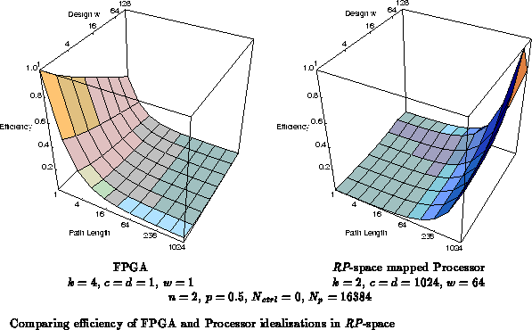
Figure shows graphically this idealized
comparison projected into RP-space in the style used in
Section
. As noted before, the FPGA is less than 1%
efficient at the cross point of wide task data words and long path lengths.
Similarly, the modeled processor is less than 1% efficient processing
single bit data items at a path length of one. Certainly, if the processor
needs to perform bit operations that do not match its special-purpose
support, the inefficiency will be at least this large -- and may be greater
due to the effects noted above which make the real processor larger than
the model.
We have already noted that RP-space is large such that we can see two or more orders of magnitude in efficiency loss when the application requirements are mismatched with the architecture structure for fixed instruction architectures. Our comparison in the previous sections underscores that the general-purpose architectural space is even larger making it paramount that one understand the realm of efficiency for each ``general-purpose'' computing device when selecting a device for an application. They underscore the room for intermediate architectures such as the DPGA, PADDI, or VDSP to cover parts of the space which are not covered well by either conventional extremes of processor or FPGAs. They also underscore the desirability of architectures like MATRIX which allow some run-time reallocation of resources to provide more robust yielded performance across the computational space.
Since many tasks have a mix of irregular and regular computing components and a mix of native data sizes, a hybrid architecture which tightly couples arrays of mixed datapath sizes and instruction depths along with flexible control may be able to provided the most robust performance across the entire application. While this thesis focussed on characterizing the implications of each pure architectural point, it should be clear from the development here how a hybrid architecture might be better suited to the mix of datasizes and regularities seen in real applications. In the simplest case, such an architecture might couple an FPGA or DPGA array into a conventional processor, allocating the regular, fine-grained tasks to the array, and the irregular, coarse-grained tasks to the conventional processor. Such coupled architectures are now being studied by several groups ( e.g. [DeH94] [Raz94] [WC96]).
In summary, we see that conventional, general-purpose device architectures, both microprocessors and FPGAs, live far apart in a rich architectural space. As feature sizes shrink and the available computing die real-estate grows, microprocessors have traditionally gone to wider datapaths and deeper instruction and data caches, while FPGAs have maintained single-bit granularity and a single instruction per array element. This trend has widened the space between the two architectural extremes, and accentuated the realm where each is efficient. A more effective use of the silicon area now becoming available for the construction of general-purpose computing components may lie in the space between these extremes. In this space, we see the emergence of intermediate architectures, architectures with flexible resource allocation, and architectures which mix components from multiple points in the space. Both processors and FPGAs stand to learn from each other's strengths. In processor design, we will learn that not all instructions need to change on every cycle, allowing us to increase the computational work done per cycle without correspondingly increasing on-chip instruction memory area or instruction distribution bandwidth. In reconfigurable device design, we will learn that a single instruction per datapath is limiting and that a few additional instructions are inexpensive, allowing the devices to cope with a wider range of computational tasks efficiently.
Over the past two decade, microprocessors have steadily increased their word size and their cache size. While these trends allow larger tasks to fit in on-chip caches and allow processors to handle larger word operations in a single cycle, the trends also make processors less and less efficient in their use of die area. While some large word operations are required, a larger and larger fraction of the operations executed by modern processors use only a small portion of the wide datapath. The computationally critical portions of programs occupy only small portions of the instruction and data cache.
We can continue to improve aggregate processor performance by using more silicon in this manner, but the performance per unit area will steadily decrease. To the extent that silicon area is inexpensive, task recompilation is hard or unacceptable, and various forms of parallelism are difficult to achieve, the current trends have their value.
However, to the extent we wish to engineer better silicon system which do more with less resources, these trends are now yielding diminishing returns. We can manage more programmable compute elements than a single, central word-wide, ALU on modern IC dies. Reconfiguration allows us to do this without paying a prohibitive costs for increased instruction distribution as we go to more, independently controlled computing units.
The conventional view of multiprocessing is that we replicate the entire microprocessor and place these replicas on the same board or die. At best, this allows aggregate performance to improve with additional area dedicated to additional processors. However, it entails a large amount of unnecessary cost, replicating entire processors when many portions of the processor may not need to be replicated. Further, coupling between processors is poor, at best, entailing 10's to 100's of cycles of latency to move data from one processing element to another and significant overhead to coordinate the activities of multiple processing units.
Most of the task which have generally been ``good'' multiprocessor
applications are very regular computing tasks for which configured,
systolic dataflow can provide more area efficient implementations. For the
sake of intuition, consider an image processing task where we need to
perform 100 operations on each pixel. We can divide this task among
conventional processors, where each processor must have memory to hold the
100 operations and must pay overhead cycles for communication, as
necessary, among the
processors. Alternately, we can configure a
hardware pipeline to process the data. If we allocate 100 compute elements,
each compute element in the configured pipeline needs to only execute its
one operation. Direct connections between computing elements transport
data avoiding additional overhead cycles. To get the same throughput as
the 100 element systolic design, the multiprocessor implementation would
need, at least, 100 processors. In terms of instruction memory alone, the
multiprocessor implementation requires memory area to hold 9900 more
instructions than the systolic implementation, making it significantly
larger just to support the same throughput.
The traditional strength of microprocessors has been their ability
to pack large computations into small area by reusing central computing
resources. This tight packing of functionality comes at the cost of a
decrease in computational density as we saw in Chapter and
Section
. When we are willing to pay area to increase
throughput, the traditional microprocessor architecture is not efficient
since it brings with it the baggage of a large investment in instruction
distribution, instruction memory, and control which are unnecessary for
highly regular tasks. Further, the i/o structure of conventional
processors is designed around heavy sequentialization, creating an
interconnect bottleneck which makes high throughput usage impractical.