Notes on Programmable Interconnect
Andre DeHon
Original Issue: February, 1995
Last Updated: Sat Apr 8 21:42:45 EDT 1995

This is a collection of notes on programmable interconnect design for reconfigurable devices. These notes were collected in the context of DPGA design (tn95) (tn114) (tn112), but are mostly relevant to FPGA design in general.
Section starts by describing the basic primitives used
for building reconfigurable interconnect. Section
describes
two extremes in reconfigurable interconnect, and Section
reviews the interconnect used in the DPGA prototype as an example.
Section
formulates a general set of design goals for
reconfigurable interconnect. Section
builds on
the concepts detailed here to formulate a general interconnection strategy
for programmable devices.
At the base of the network topology we consider two main interconnect primitives: multiplexors and crossbars.
Multiplexors -- Multiplexors select a signal from one of several
input signals. Here, several lines in the programmable interconnect are
brought into the data inputs of the mux and the context configuration
drives the selector input to the mux as shown below. The configuration
memory has multiple contexts as with the array element (gate) memory (See
Figure ).
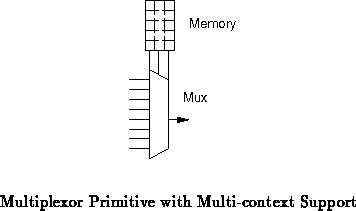
It may be instructive to compare this primitive to the LUT (lookup table) used for the logical gate primitive in many reconfigurable devices ( e.g. [Xil93] [BCE +94]). In the gate case, the inputs (from the programmable network) connect into the selector and the configuration (from the context memory) connects into the data inputs of the mux. In the interconnect case, functions are swapped with the inputs driving into the data inputs of the mux, and the configuration memory driving into the selector inputs.
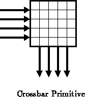
Crossbars -- A crossbar is a basic interconnect primitive with a set of
inputs and a set of outputs which can connect any of its outputs to any of
its inputs (See Figure ). One could, for instance, build an
(
inputs,
outputs) crossbar by taking
,
-input mux
primitives as introduced above and wiring the inputs on each of the muxes
together.
Other programmable interconnect primitives exist, such as:
For example, consider the crossbar. It contains
switches. If a memory cell were dedicated to each switch, it would require
memory cells per context. However, if we restrict the sensible
configurations to those which connect each output to exactly one input, the
legal space of configurations is only
. If the crossbar
primitive is built out of the mux primitive as suggested above, we require
exactly
memory cells per context. This savings in
configuration memory is, of course, of increasing importance as we go to
larger numbers of on-chip contexts.
It is worth noting that, even with crossbars and multiplexors, one can
build systems where multiple, ``distinct'' configurations are functionally
equivalent. For these reasons, one needs to consider the entire system and
what configurations are logically distinct. Consider, for example, using
an crossbar to select the 4 inputs to a 4-LUT. Since all the
inputs to the 4-LUT are logically equivalent (assuming we have freedom to
fully program the LUT memory), the order of the input signals into the
4-LUT does not matter. That is, all
combinations of a given subset
of 4 inputs will be equivalent. It, therefore, does not make sense to use
a crossbar in this case. In fact, the crossbar has
configurations whereas only
combinations are distinct in this scenario. As a
consequent, it is generally better to use multiplexors for the final
input selection into a LUT than using a crossbar.
The key idea here is to match the information content stored in
configuration memory to the information content required to configure all
interesting and distinct configurations of the programmable device. In
particular, if a device can be configured in legal and useful ways, it
should only require
bits of memory to specify its
configuration.
Now, let's look at the first two schemes for network interconnect which may come to mind:
Full Crossbar -- In the most extreme case of full connectivity, we could build a full crossbar to connect every array element input to every array element output. In such a scheme we would not have to worry about whether or not a given network could be mapped onto the programmable interconnect -- however, the cost for this full interconnect is prohibitively high. Further, this scheme is inefficient due to the logically equivalent configuration problem introduced above.
For an element array where each element is a
-input function (
e.g.
-LUT), the crossbar would be a
crossbar. This requires
memory bits for
configuration. Arranged in a roughly square array, each input and output
must travel
distance, before we account for saturated wire
density. Since interconnect delay is proportional to interconnect
distance, this implies the interconnect delay grows at least as
. However, the bisection bandwidth for this crossbar
.
For sufficiently large
, this bisection bandwidth requires that the side
of an array be
to accommodate the wires across the bisection. In
turn, the
bisection bandwidth dictates an area
and input
and output runs of length
. For large crossbars, then,
wire size dominates the active logic and the configuration space.
Full crossbars make some pragmatic sense in the region where the
interconnect requirements (which grow as ) and configuration
requirements (which grow as
) do not dominate the logical
array size (which grows as
). In this region where size is dominated
by the array element logic, interconnect delays grow as
, so
size is still balanced with the mandatory interconnect delay.
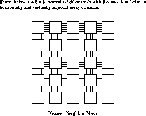
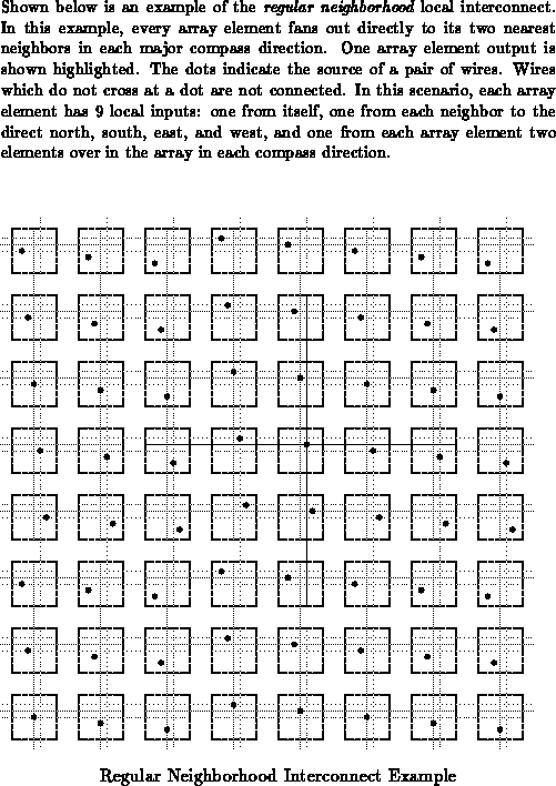
Nearest Neighbor or mesh -- At the opposite extreme, we can use
only local connections within the mesh between adjacent (or close) array
elements. By limiting all the connections to fixed distances, the link
delay does not grow as the array grows. Further, the bisection bandwidth
in a mesh configuration is and hence, never dominates the
logical array element size. However, communicating a piece of data between
two points in the array requires switching delay proportional to the
distance between the source and the destination. Since switching delay
through programmable interconnect is generally much larger than fanout or
wire propagation delay along a fixed wire, this makes distant communication
slow and expensive. For example, in a topology where direct connections
are only made between an array element and its north, east, south, and west
neighbors (typically called a NEWS network -- See Figure
), a
signal must traverse a number of programmable switching elements
proportional to the Manhattan distance between the source and the
destination (
). For the interconnect network topologies
typically encountered in logic circuits, this can make interconnect delay
quite high -- easily dominating the delay through the array element logic.
The DPGA prototype (tn114) (tn112) uses a two-tiered
interconnect scheme. The array elements are organized into small arrays
(subarrays) which are, in turn, tiled to build the entire array. The
subarray acts as the leaf of the interconnect hierarchy. Each array
element output is run vertically and horizontally across the entire span of
the subarray. Each array element can, in turn, select as an input the
output of any array element in its subarray which shares the same row or
column (See Figure ). This topology allows a reasonably high
degree of local connectivity without incurring the delay costs of switching
through additional interconnect.
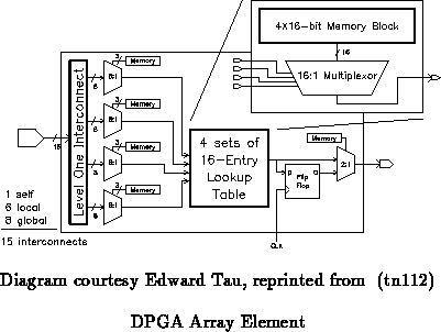
In addition to the local outputs which run across each row and column, a
number of non-local lines are also allocated to each row and column. The
non-local lines are driven by the global interconnect. Each LUT can then
pick inputs from among the lines which cross its array element (See
Figures and
). In the prototype, each
row and column support four non-local lines. Each array element can thus
pick its inputs from eight global lines, six row and column neighbor
outputs, and its own output. Each input is configured with an 8:1
multiplexor taping from a subset of the 15 lines into each cell for the
reasons suggested above. Of course, not all combinations of 15 inputs
taken 4 at a time are available with this scheme. The inputs are arranged
so any combination of local signals can be selected along with many subsets
of global signals. Freedom available at the crossbar in assigning global
lines to tracks reduces the impact of this restriction.
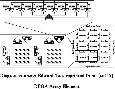
Between each subarray a pair of crossbars route the subarray outputs from
one subarray into the non-local inputs of the adjacent subarray (See
Figure ). Note that all array element outputs are
available on all four sides of the subarray. In our prototype, this means
that each crossbar is a 16
8 crossbar which routes 8 of the 16
outputs to the neighboring subarray's 8 inputs on that side. Each
16
8 crossbar is backed by a 4
32 memory to provide the 4
context configurations. Each crossbar output is configured by decoding 4
configuration bits to select among the 16 crossbar input signals.
While the nearest neighbor interconnect is minimally sufficient for the
33 array in the prototype, a larger array should include a richer
interconnection scheme among subarrays to avoid incurring a large switching
delay when routing between distant subarrays.
See [BCE +94] for more details of the prototype interconnect.
After seeing these examples, we can begin to formulate the design requirements for our programmable interconnect:
Following from the above, we can formulate a general family of interconnection networks which looks most promising. This family has multiple levels of interconnect like the prototype. Unlike the prototype, they may have more than one level of non-local interconnect. Several viable interconnect topologies exist for each of the levels of interconnect and their composotion.
At the base, of the interconnect hierarchy, there are local connections among array elements. These are generally worth keeping in any scheme because:
Some viable local interconnect schemes include:
Beyond the local interconnect, we need to wire up logical elements which must be placed further apart and provide for larger fanout. This is best done by integrating additional levels of network on top of the local interconnect.
The first issue to address is interfacing between the local and non-local interconnect. To receive non-local signals, the local network usually allocates some input channels to routed, non-local signals. For instance, a local crossbar scheme might increase the number of inputs on the crossbar to receive several non-local signals in addition to the local signals. In the prototype, the local multiplexors which delivered inputs to each LUT tapped off of both local and non-local tracks which span each column. In general, the non-local interconnect would arrange to switch a few non-local signals into the local network input and the local network would take care of routing these signals to the array elements themselves.
Conversely, we need to get the array element outputs into the non-local network. Typically, this is done by selecting an interesting subset of the local signals to concentrate into the non-local network and is often integrated with the first-level of the non-local interconnect. In the prototype, all the local outputs from a subarray were brought into a crossbar which then selected a subset and switched them into the non-local inputs to the adjacent subarray.
The topology for the non-local network is likely to draw upon many of the basic topologies we've already introduced. At the same time, it is likely to be organized into a hierarchically structure where a series of non-local networks are layered on top of each other, each spanning a successively larger portion of the array.
A given level of the non-local interconnect, then might be:
Of course, the bandwidth handled in the successive stages of the network must be carefully chosen. If the bandwidth is chosen too high, the higher level network will occupy more space than can be fruitfully employed. If chosen too low, it won't be possible to route all the desired, long-distance connections using the hierarchical interconnect.
Since they are layered on top of each other in 2-space on the IC die, the bisection bandwidth from all levels composes to determine the bisection bandwidth of the device. If a geometric scheme is chosen where each level in the hierarchy supports a bisection bandwidth which is a fraction of the total bisection bandwidth of its constituency, the total bisection bandwidth is only a constant multiple of the base bisection bandwidth.
e.g. Consider the nearest-neighbor mesh with 4 connections in each
compass direction. Now consider that each group of neighbors is
grouped into a level 1 node, each group of
level 1 nodes are
grouped into a level 2 node, and so on. Further, assume the aggregate
level-n bandwidth between nearest neighbors is one-half the total bandwidth
at lower levels. So, the level-1 nodes have
nearest
neighbor connections, and the level-2 nodes have
nearest neighbor connections. Viewing this in an amortized sense at each
array element, the total bandwidth in each compass direction is
or,
, in the limit of infinitely many levels of interconnect.
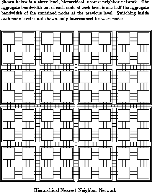
In fact, in general, if the bandwidth between nodes at level in the
hierarchy is one
-th the total bandwidth of the contained level
interconnect between nodes, the total bisection bandwidth will be
times the base bisection bandwidth. Note that this result
is independent of the size of the array, so this topology scales nicely
to larger arrays.
At upper levels of the network, the nearest neighbor network should provide corner turns and selective spanning, neither of which were necessary for the local nearest-neighbor connections.
While not identical in formulation or breadth, this topology captures the essence of mesh with bypass interconnect, segmented channel routing, and express cubes [Dal91].
For simplicity, I have described composite networks which are homogeneous in both organization and style. However, that need not be the case. The node size or bandwidth may want to change between levels within the same style, and it may be beneficial to mix styles. For example, local, crossbar subarrays may be interconnected by regular neighborhoods of interconnect which are in turn connected by nearest neighbor connections.
Since switching delays in the interconnect can be comparable to logic delays, it will often make sense to pipeline the transmission of data through long interconnect. In particular, it may be useful to use the array element logic plus local interconnect delay as a base cycle time. When connections need to traverse additional, hierarchical interconnect, this will entail larger delay. By pipelining across these interconnect, we can operate at the base cycle time despite the larger latency in the interconnect. Here it will make sense to group a number of switching stages together whose delay is comparable to the array element logic plus local interconnect delay and treat each such group as a separate pipeline stage. Programmable or manditory flip-flops associated with the switching network will be needed support the pipelined interconnect discipline.
When we include the multiple context configurations which switch the interconnect, we can also time-multiplex each piece of interconnect. This works especially well with the pipeline interconnect. Cycled at the base cycle time the interconnect can pipeline multiple bits of data, potentially destined for different destinations, across any individual wire during the switching latency required to get a bit between distant portions of the device. This time-multiplexed wire use allows one to extract the full bandwidth of the wires on the programmable device, allowing much higher utilization than when a single signal is statically associated with each wire in the programmable interconnect. Note that this exploits the same basic characteristics as Virtual Wires [BTA93], but inside the programmable device.
Since the delay, density, and area constants associated with off-chip interconnect is substantially different from on-chip interconnect ( i.e. it is much slower, less dense, and larger), it often makes sense to handle device i/o specially in the network. To avoid periphery pin limitations, it may make sense to drive inputs directly into higher level, long-spanning interconnect in the array rather than simply into peripheral, nearest neighbor connections. Similarly, output connections may want to come from higher, coarser levels in the hierarchical interconnect rather than from local interconnect. Further, techniques like time-multiplexing the i/o pins to maximize their bandwidth ( e.g. Virtual Wires) are generally beneficial.