MATRIX:
A Reconfigurable Computing Architecture with
Configurable Instruction Distribution
and Deployable Resources
Ethan Mirsky
Andre DeHon
Original Issue: December, 1995
Last Updated: Thu Jul 4 21:35:43 EDT 1996

MATRIX is a novel, coarse-grain, reconfigurable computing
architecture which supports configurable instruction distribution. Device
resources are allocated to controlling and describing the computation on a
per task basis. Application-specific regularity allows us to compress the
resources allocated to instruction control and distribution, in many
situations yielding more resources for datapaths and computations. The
adaptability is made possible by a multi-level configuration scheme, a
unified configurable network supporting both datapaths and instruction
distribution, and a coarse-grained building block which can serve as an
instruction store, a memory element, or a computational element. In a
0.5 CMOS process, the 8-bit functional unit at the heart of the MATRIX
architecture has a footprint of roughly 1.5mm
1.2mm, making single dies
with over a hundred function units practical today. At this process point,
100MHz operation is easily achievable, allowing MATRIX components to
deliver on the order of 10 Gop/s (8-bit ops).
General-purpose computing architectures must address two important questions:
Most of the area on a modern microprocessor goes into storing data and instructions and into control circuitry. All this area is dedicated to allowing computational tasks to heavily reuse the small, active portion of the silicon, the ALUs. Consequently, very little of the capacity inherent in a processor gets applied to the problem - most of it goes into supporting a large operational diversity. Further, the rigid word-SIMD ALU instructions coupled with wide processor words make processors relatively inefficient at processing bit or byte-level data.
Conventional Field Programmable Gate Arrays (FPGAs) allow finer granularity control over operation and dedicate minimal area to instruction distribution. Consequently, they can deliver more computations per unit silicon than processors on a wide range of regular operations. However, the lack of resources for instruction distribution make them efficient only when the functional diversity is low --- i.e. when the same operation is required repeatedly and that entire operation can be fit spatially onto the FPGA or FPGAs in the system.
Dynamically Programmable Gate Arrays (DPGAs) [TEC +95] [DeH96] dedicate a modest amount of on-chip area to store additional instructions allowing them to support higher operation diversity than traditional FPGAs. The area necessary to support this diversity must be dedicated at fabrication time and consumes area whether or not the additional diversity is required. The amount of diversity supported -- i.e. the number of instructions -- is also fixed at fabrication time. Further, when regular datapath operations are required many instruction stores will be programmed with the same data.
Rather than separate the resources for instruction storage and distribution from the resources for data storage and computation and dedicate silicon resources to them at fabrication time, the MATRIX architecture unifies these resources. Once unified, traditional instruction and control resources are decomposed along with computing resources and can be deployed in an application-specific manner. Chip capacity can be deployed to support active computation or to control reuse of computational resources depending on the needs of the application and the available hardware resources.
In this paper we introduce the MATRIX architecture. The following
section (Section ) provides an overview of the basic
architecture. In Section
, we show usage examples to illustrate
the architecture's flexibility in adapting to varying application
characteristics. Section
puts MATRIX in context with some
of its closest cousins. We comment on MATRIX's granularity in
Section
. In Section
, we highlight
implementation characteristics from our first prototype.
Section
concludes by reviewing the key aspects of the MATRIX
architecture.
MATRIX is composed of an array of identical, 8-bit functional units
overlayed with a configurable network. Each functional unit contains a
2568-bit memory, an 8-bit ALU and multiply unit, and reduction
control logic including a 20
8 NOR plane. The network is
hierarchical supporting three levels of interconnect. Functional unit port
inputs and non-local network lines can be statically configured or
dynamically switched.
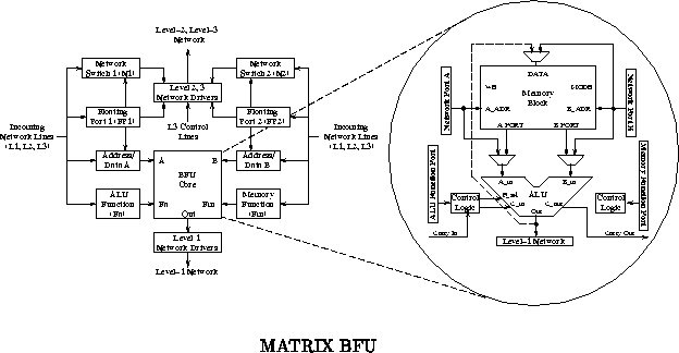
The Basic Functional Unit (BFU) is shown in Figure .
The BFU contains three major components:
MATRIX operation is pipelined at the BFU level with a pipeline register at each BFU input port. A single pipeline stage includes:
The BFU can serve in any of several roles:
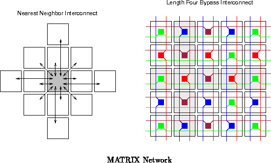
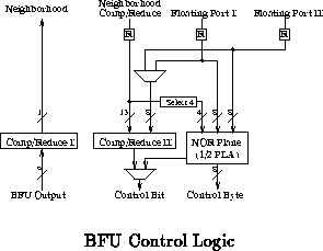
The MATRIX network is a hierarchical collection of 8-bit busses. The interconnect distribution resembles traditional FPGA interconnect. Unlike traditional FPGA interconnect, MATRIX has the option to dynamically switch network connections. The network includes:
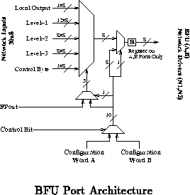
The MATRIX port configuration is one of the keys to the
architecture's flexibility. Figure shows the composition
of the BFU network and data ports. Each port can be configured in one of
three major modes:
For illustrative purposes, let us consider various convolution
implementations on MATRIX. Our convolution task is as follows:
Given a set of weights {
,
, ...
} and a sequence of
samples {
,
,
}, compute a sequence of results
{
,
,
} according to:
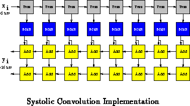
Figure shows an eight-weight (
) convolution of 8-bit
samples accumulating a 16-bit result value. The top row simply carries
sample values through the systolic pipeline. The middle row performs an
8
8 multiply against the constants weights,
's, producing a
16-bit result. The multiply operation is the rate limiter in this task
requiring two cycles to produce each 16-bit result. The lower two rows
accumulate
results. In this case, all datapaths (shown with arrows
in the diagram) are wired using static source mode (Figure
).
The constant weights are configured as static value sources to the
multiplier cells. Add operations are configured for carry chaining to
perform the required 16-bit add operation. For a
-weight filter, this
arrangement requires
cells and produces one result every 2 cycles,
completing, on average,
8
8 multiplies and
16-bit adds per cycle.
In practice, we can:
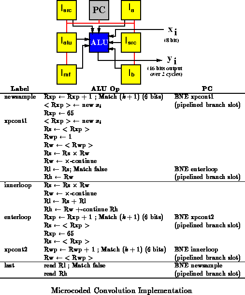
Figure shows a microcoded convolution implementation. The
coefficient weights are stored in the ALU register-file memory in
registers 1 through
and the last
samples are stored in a ring buffer
constructed from registers 65 through
. Six other memory location
(Rs, Rsp, Rw, Rwp, Rl, and Rh) are used to hold values during the
computation. The ALU's A and B ports are set to dynamic
source mode. I-store memories are used to drive the values controlling the
source of the A and B input (two
memories), the values fed into
the A and B inputs (
,
), the memory function (
) and
the ALU function (
). The PC is a BFU setup to increment its
output value or load an address from its associated memory.
The implementation requires 8 BFUs and produces a new 16-bit result
every cycles. The result is output over two cycles on the ALU's
output bus. The number of weights supported is limited to
by the
space in the ALU's memory. Longer convolutions (larger
) can be
supported by deploying additional memories to hold sample and coefficient
values.
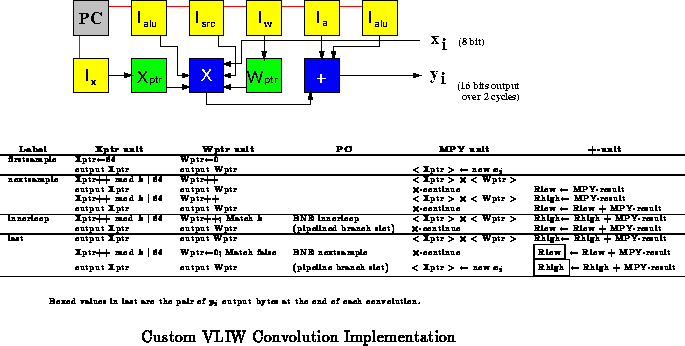
Figure shows a VLIW-style implementation of the convolution
operation that includes application-specific dataflow. The sample pointer
(Xptr) and the coefficient pointer (Wptr) are each given a BFU, and separate
ALUs are used for the multiply operation and the summing add operation.
This configuration allows the inner loop to consist of only two operations,
the two-cycle multiply in parallel with the low and high byte additions.
Pointer increments are also performed in parallel. Most of the I-stores
used in this design only contain a couple of distinct instructions.
With clever use of the control PLA and configuration words, the number of
I-stores can be cut in half making this implementation no more costly than
the microcoded implementation.
As shown, the implementation requires 11 BFUs and produces a new
16-bit result every cycles. As in the microcoded example the result
is output over two cycles on the ALU output bus. The number of weights
supported is limited to
by the space in the ALU's memory.
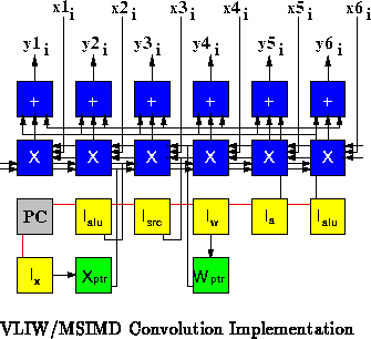
Figure shows a Multiple-SIMD/VLIW hybrid implementation based
on the control structure from the VLIW implementation. As shown in the
figure, six separate convolutions are performed simultaneously sharing the
same VLIW control developed to perform a single convolution, amortizing the
cost of the control overhead. To exploit shared control in this manner,
the sample data streams must receive data at the same rate in lock step.
When sample rates differ, separate control may be required for each different rate. This amounts to replicating the VLIW control section for each data stream. In the extreme of one control unit per data stream, we would have a VLIW/MIMD implementation. Between the two extremes, we have VLIW/MSIMD hybrids with varying numbers of control streams according to the application requirements.
Of course, many variations on these themes are possible. The power of the MATRIX architecture is its ability to deploy resources for control based on application regularity, throughput requirements, and space available. In contrast, traditional microprocessors, VLIW, or SIMD machines fix the assignment of control resources, memory, and datapath flow at fabrication time, while traditional programmable logic does not support the high-speed reuse of functional units to perform different functions.
Owing to the coarse-grain configurability, the most closely related architectures are PADDI [CR92], PADDI-2 [YR95], and PMEL's vDSP [Cla95]. PADDI has 16-bit functional units with an 8-word deep instruction memory per processing element. A chip-wide instruction pointer is broadcast on a cycle-by-cycle basis giving PADDI a distinctly VLIW control structure. From what little public information is available, the vDSP appears to have a similar VLIW control structure with 4 contexts and 8-bit wide functional units. PADDI-2 also supports 8 distinct instructions per processing element but dispenses with the global instruction pointer, implementing a dataflow-MIMD control structure instead. While the MATRIX BFU is similar in functional composition to these devices, MATRIX is unique in control flexibility, allowing the control structure, be it SIMD, VLIW, MIMD, systolic, or a hybrid structure, to be customized on a per application basis.
Dharma [BCK93], DPGA [TEC +95], and VEGA [JL95] demonstrate various fixed design points with dedicated context memory for reusing the computing and interconnect resources in fine-grained programmable arrays. Dharma has a rigid decomposition of resources into computational phases. The DPGA provides a more flexible multicontext implementation with a small context memory ( e.g. 4 in the prototype). At the other end of the spectrum, VEGA has 2048 context memory words. The differences in these devices exhibit the tension associated with making a pre-fabrication partitioning and assignment of resources between instruction memory, data memory, and active computing resources. While necessarily granular in nature, MATRIX allows the resource assignment to be made on a per application basis.
The proposed DP-FPGA [CL94] controls multiple FPGA LUTs or interconnect primitives with a single instruction. However, the assignment of instructions to functional units, and hence the width of the datapath of identically controlled elements is fixed at fabrication time. MATRIX allows a single control memory to control multiple functional units simultaneously in a configurable-SIMD fashion. This provides a form of instruction memory compression not possible when instruction and compute resources have fixed pairings.
As seen in Section , MATRIX can be configured to operate in
VLIW, SIMD, and MSIMD fashion. Unlike traditional devices, the arrangement
of units, dataflow, and control can be customized to the application. In
the SIMD cases, MATRIX allows the construction of the master control and
reduction networks out of the same pool of resources as array logic,
avoiding the need for fixed control logic on each chip or an off-chip array
controller. Like MSIMD ( e.g. [Nut77][Bri90]) or
MIMD multigauge [Sny85] designs,
the array can be broken into units operating on different instructions.
Synchronization between the separate functions can be lock-step VLIW, like
the convolution example, or completely orthogonal depending on the
application. Unlike traditional MSIMD or multigauge designs, the control
processors and array processors are built out of the same building block
resources and networking. Consequently, more array resources are available
as less control resources are used.
To handle mixed granularity data efficiently, a number of architectures
have been proposed or built which have segmentable datapaths ( e.g.
[Sny85] [BSV +95]). These generally exhibit
SIMD instruction control for the datapath, but can be reconfigured to treat
the bit datapath as
,
-bit words, for certain,
restricted, values of
. Modern multimedia processors ( e.g.
[Sla95] [Eps95]) allow the datapath to be treated as
a collection of 8, 16, 32, or 64 bit words. MATRIX handles mixed or varying
granularities by composing BFUs and deploying instruction control. Since
the datapath size and assignment of control resources is not fixed for a
MATRIX component, MATRIX has greater flexibility to match the datapath
composition and granularity to the needs of the application.
The LIFE [LS90] VLIW architecture was designed to allow easy synthesis of function-specific micro-programmed architectures. The number and type of the functional units can be varied prior to fabrication. The control structure and resources in the architecture remain fixed. MATRIX allows the function-specific composition of micro-programmed functional units, but does not fix control or resource allocation prior to fabrication time.
Reviewing the microcoded example in Section , we can see both
how microprocessors manage to achieve more functional diversity than FPGAs
and how FPGAs and other reconfigurable architectures can achieve higher
performance than processors on highly repetitive computing tasks with
limited functional diversity. In order to support heavy reuse of a
functional unit, a considerable fraction of the resources must go into
controlling the functions and datapaths including the memory to hold
programs and data, as we see in the microcoded example. This is one of the
primary reasons that the performance provided by microprocessors is small
compared to their reconfigurable counterparts - most of the device
capacity in microprocessors is dedicated to memory and control not to
active computation required by the task. Furthermore, in cases such as
this one, most of the cycles on the active resources are dedicated to
control and bookkeeping.
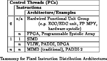
Table presents an instruction stream taxonomy for
multiple data computing devices. Owing to their fixed instruction control
structure, all traditional computing devices can be categorized in this
taxonomy. MATRIX is unique in that its multi-level configuration allows
it, post fabrication, to implement any of these structures and many hybrids.
Independent of an application configuration, MATRIX defies strict
classification based on the number of instructions and threads of control.
The 8-bit granularity used in MATRIX is a convenient size for use in datapaths, memory addressing, and control. Using the configurable instruction distribution, wide-word operations can be cascaded with reasonable efficiency. The overhead for configuring and controlling datapaths is significantly reduced compared to a bit-level network configuration. Owing to the 8-bit granularity, MATRIX will not completely subsume bit-granularity reconfigurable devices for irregular, fine-grained operations.
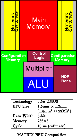
Figure shows the composition of a BFU along with its size
and performance. As described in Section
, the BFU is pipelined
at the BFU level allowing high speed implementation. The 10 ns cycle
estimate is for the university prototype. With only a small memory read,
an ALU operation, and local network distribution, the basic cycle rate can
be quite small -- at least comparable to microprocessor clock rates.
The area breakdown is roughly: 50% network, 30% memory, 12% control, and
8% ALU including the multiplier. At 1.8mm
, 100 BFUs fit on a
17mm
14mm die. A 100 BFU MATRIX device operating at 100MHz has a
peak performance of
8-bit operations per cycle (10 Gop/s).
Traditional computing devices are configured for an application by their instruction stream. However, the composition of their instruction stream and the resources it occupies cannot be tailored to the application. With a multi-level configuration scheme, MATRIX allows the application to control the division of resources between computation and control. In the process, MATRIX allows the application to determine the specifics of the instruction stream. Consequently, MATRIX to provide: