DPGA Utilization and Application
Andre DeHon
Original Issue: September, 1995
Last Updated: Fri May 17 20:10:30 EDT 1996
Dynamically Programmable Gate Arrays (DPGAs) are programmable arrays which allow the strategic reuse of limited resources. In so doing, DPGAs promise greater capacity, and in some cases higher performance, than conventional programmable device architectures where all array resources are dedicated to a single function for an entire operational epoch. This paper examines several usage patterns for DPGAs including temporal pipelining, utility functions, multiple function accommodation, and state-dependent logic. In the process, it offers insight into the application and technology space where DPGA-style reuse techniques are most beneficial.
FPGA capacity is conventionally metered in terms of ``gates'' assigned to a problem. This notion of gate utilization is, however, a purely spatial metric which ignores the temporal aspect of gate usage. That is, it says nothing about how often each gate is actually used. A gate may only perform useful work for a small fraction of the time it is employed. Taking the temporal usage of a gate into account, we recognize that each gate has a capacity defined by its bandwidth. Exploiting this temporal aspect of capacity is necessary to extract the most performance out of reconfigurable devices.
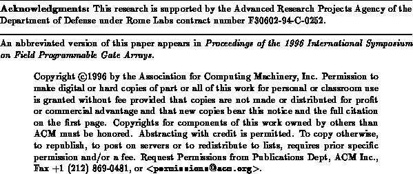
To first order, conventional FPGAs only fully exploit their
potential gate capacity when fully pipelined to solve a single task with
data processing rates that occupy the entire array at its maximum clock
frequency. In the extreme, each pipeline stage contains a minimum amount
of logic and interconnect (See Figure ). As task requirements
move away from this extreme, gates are used at a fraction of their
potential capacity and FPGA utilization efficiency drops.
Away from this heavily pipelined extreme, multiple context devices, such as DPGAs, provide higher efficiency by allowing limited interconnect and logic element resources to be reused in time. These devices allow the temporal component of device capacity to be deployed to increase total device functionality rather than simply increasing throughput for fixed functionality.
In this paper we examine several, stylized usage patterns for DPGAs
focusing on the resource reuse they enable. We start by identifying
capacity and utilization metrics for programmable devices
(Section ). We examine a few characteristics of application and
technology trends (Section
) to understand why resource reuse is
important. In Section
we briefly review DPGA characteristics
and look at the costs for supporting resource reuse. The heart of the
paper then focuses on four broad styles for resource reuse:
An FPGA is composed of a number of programmable gates interconnected by
wires and programmable switches. Each gate, switch, and wire has a limited
bandwidth () --- or time between uses
(
) necessary for correct operation. In a unit
of time
, we could, theoretically, get a maximum of
gate evaluations, and
switch and wire traversals.
Each gate, switch, and wire has an inherent propagation latency
() as well.
For simplicity, let us model an FPGA as having a single, minimum reuse time,
, which is the minimum reuse time for a gate evaluation and
local interconnect. We will assume
captures both the
bandwidth and the propagation delay limitations. The flip-flop toggle rate
which was often quoted by vendors as a measure of device performance
[Xil94], provides a rough approximation of
for commercial devices ( i.e.
). Throughout, we assume
to allow simple
time discretization and comparison.
The peak operational capacity of our FPGA is thus:
may be any of the potentially limited device resources such
as gates, wires, or switches.
This peak capacity is achieved when the FPGA is clocked at
and every gate is utilized.
In our conventional model, that means every gate registers its output, and
there is at most one logic block between every pair of flip flops (See
Figure
). This is true even when the register overhead time
is not small compared to
, but the computation latency may
be increased noteably in such a case.
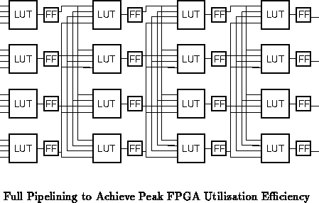
When we run at a slower clock rate to handle deeper logic paths, or the
device goes unused for a period of time, we get less capacity out of our
FPGA. Running at a clock rate
, we realize a
gate utilization:
As and
, the
utilization is below capacity. For example, if the path delay between
registers is four gate-interconnect delays (See Figure
),
such that
, even if all the device gates
are in use, the gate utilization,
, is one-quarter the peak
capacity
. more_utilization.tex
Utilization of a resource is only important to the extent that one is capacity limited in that resource. For example, if an FPGA has a plethora of gates, but insufficient switching to use them, gate utilization is irrelevant while switch utilization is paramount. When one resource is limited, pacing the performance of the system, we say this resources is the bottleneck. To improve performance we deploy or redeploy our resources to utilize the bottleneck resource most efficiently. In this section we look at the effects of bottlenecks arising from application requirements and from technology-oriented resource costs.
The first question to ask is: ``Why do we not fully pipeline every design and run it at the maximum clock frequency?'' The primary answer, aside from design complexity, is that we often do not need that much of every computation. While heavy pipelining gets the throughput up for the pipelined design, it does not give us any more functionality, which is often the limiter at the application level.
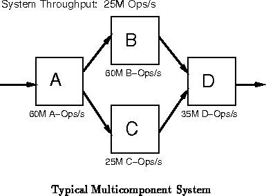
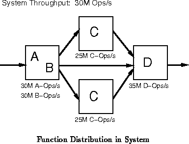
In these situations, reuse of the active silicon area on the
non-bottleneck components can improve performance or lower costs. If we
are getting sufficient performance out of the bottleneck resource, then one
may be able to reduce cost by sharing the gates on the non-bottleneck
resources between multiple ``components'' of the original design (See
Figure ). If we are not getting sufficient performance
on the bottleneck resource and its task is parallelizable, we may be able
to employ underused resources on the non-bottleneck components to improve
system performance without increasing system cost (See
Figure
).
Many bottlenecks arise from implementation technology costs. Resources which are relatively ``expensive'' in area, have inherently high latencies, or have inherently low bandwidths tend to create bottlenecks in designs. I/O and wiring resources often pose the biggest, technology-dictated bandwidth limitations in reconfigurable systems.
When data throughput is limited by I/O bandwidth, we can reuse the internal resources to provide a larger, effective, internal gate capacity. This reuse decrease the total number of devices required in the system. It may also help lower the I/O bandwidth requirements by grouping larger sets of interacting functions on each IC.
Some designs are limited by latency not bandwidth. Here, high bandwidth may be completely irrelevant or, at least, irrelevant when it is higher than the reciprocal of the design latency. This is particularly true of applications which must be serialized for correctness ( e.g. atomic actions, database updates, resource allocation/deallocation, adaptive feedback control).
By reusing gates and wires, we can use device capacity to implement these latency limited operations with less resources than would be required without reuse. This will allow us to use smaller devices to implement a function or to place more functionality onto each device.
Some computations have cyclic dependencies such that they cannot continue
until the result of the previous computation is known. For example, we
cannot reuse a multiplier when performing exponentiation until the previous
multiply result is known. Finite state machines (FSMs) also have the
requirement that they cannot begin to calculate their behavior in the next
state, until that state is known. In a purely spatial implementation, each
gate or wire performs its function during one period and
sits idle the rest of the cycle. Resource reuse is the most beneficial way
to increase utilization in cases such as these.
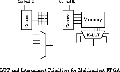
In multicontext FPGAs, we increase utilization, , by allocating space
on chip to hold several configurations for each gate or switch. Rather
than having a single configuration memory, each Look Up Table (LUT) or
multiplexor, for instance, has a small local memory (See
Figure
). A broadcast context identifier tells each primitive
which configuration to select at any given point in time.
By allocating additional memory to hold multiple configurations,
we are reducing the potential for a fixed amount of silicon. At
the same time, we are facilitating reuse which can increase utilization.
Multiple contexts are beneficial to the extent that the additional
space for memory creates a net utilization increase.
Let us consider our array as composed of context memory occupying a
fraction of the die and active area occupying
. For
simplicity, we assume
. We can now relate the
multicontext peak to the single-context FPGA peak:
We can calculate multicontext gate utilization, for example:
We can calculate an efficiency for the use of active multicontext resources:
Alternately, we can compare total silicon utilization efficiency to the single context case:
Equation computes the net utilization efficiency of the
silicon. This is the quantity we need to maximize to get the most capacity
out of our silicon resources.
Breaking up the area by number of contexts, :
In Equation , we use
instead of
since
we assume base silicon usage (
) includes one configuration and
any fixed overhead associated with it.
is the incremental cost
of one context configuration's worth of memory. To the extent the size of
the context configuration is linear in the size of the device, we can
approximate
as proportional to
:
This gives us:
or
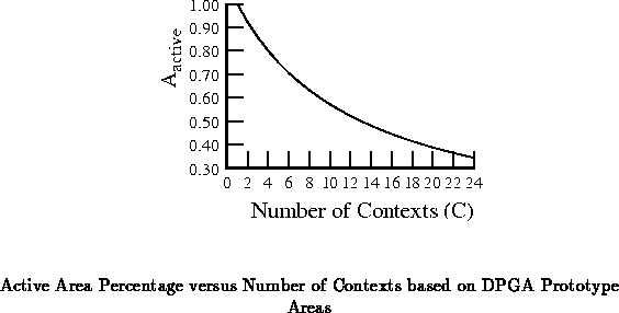
Our first generation DPGA prototype [TEC +95a] was implemented in
a 3-layer metal, 1.0m CMOS process. The prototype used 4-LUTs for the
basic logic blocks and supported 4 on-chip context memories. Each context
fully specified both the interconnect and LUT functions. Roughly 40% of
the die area consumed on the prototype went into memory. We estimate that
half of that area is required for the first context, while the remaining
area is consumed by the additional three contexts. For the prototype
implementation, then,
20% and
80%.
Based on the relative sizes in the prototypes and using the above
relations, this gives
(
,
,
,
). With these
technology constants, Equation
becomes:
Figure plots the relationship shown in
Equation
.
Context switch overhead associated with reading new configuration data
can further decrease multicontext capacity by increasing
over
. Our experience suggests that
unpipelined context changes yield a
.
This effect can be minimized by pipelining the context read at the cost of
the additional area for a bank of context registers (lowering
). We make the pedagogical assumption that
for this discourse.
The easiest and most mundane way to increase the utilization on an FPGA
is to use the FPGA for multiple, independent functions. At a very coarse
granularity, conventional FPGAs exploit this kind of reuse. The essence of
reconfigurable resources is that they do not have to be dedicated to a
single function throughout their lifetime. Unfortunately, with
multi-millisecond reconfiguration time scales, this kind of reconfiguration
is only useful in pushing up utilization in the coarsest or most extreme
sense. Since conventional devices do not support background configuration
loads, the active device resources are idle and unused during these long
reconfiguration events. Reload time thus contributes to
(Equation
).
With multiple, on-chip contexts, a device may be loaded with several
different functions, any of which is immediately accessible with minimal
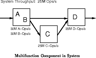
overhead. A DPGA can thus act as a ``multifunction peripheral,''
performing distinct tasks without idling for long reconfiguration
intervals. In a system such as the one shown in Figure ,
a single device may perform several tasks. When used as a reconfigurable
accelerator for a processor ( e.g. [AS93]
[DeH94a] [RS94]) or to implement a dynamic
processor ( e.g. [WH95]), the DPGA can support multiple
loaded acceleration
functions simultaneously. The DPGA provides greater capacity by allowing
rapid reuse of resources without paying the large idle-time overheads
associated with reconfiguration from off-chip memory.
In a data storage or transmission application, for instance, one may be limited by the network or disk bandwidth. A single device may be loaded with functions to perform:
Within a CAD application, such as espresso [RSV87], one needs to perform several distinct operations at different times, each of which could be accelerated with reconfigurable logic. We could load the DPGA with assist functions, such as:
Some classes of functionality are needed, occasionally but not continuously. In conventional systems, to get the functionality at all, we have to dedicate wire or gate capacity to it, even though it may be used very infrequently. A variety of data loading and unloading tasks fit into this ``infrequent use'' category, including:
In a multicontext DPGA, the resources to handle these infrequent cases can be relegated to a separate context, or contexts, from the ``normal'' case code. The wires and control required to shift in (out) data and load it are allocated for use only when the respective utility context is selected. The operative circuitry then, does not contend with the utility circuitry for wiring channels or switches, and the utility functions do not complicate the operative logic. In this manner, the utility functions can exist without increasing critical path delay during operation.
A relaxation algorithm, for instance, might operate as follows:
In the introduction we noted that we can extract the highest capacity
from our FPGAs by fully pipelining every operation. When we need the highest
throughput for the task, but limited functionality, this technique
works well. However, we noted in Section that application and
technology bottlenecks often limited the rate at which we could provide new
data for a design such that this maximum throughput is seldom necessary.
Further, we noted that many applications are limited in the amount of
distinct functionality they provide rather than the amount of throughput for
a single function. Temporal pipelining is a stylized way of organizing
designs for multi-context execution which uses available capacity
to support a larger range of functions rather than providing more
throughput for a single piece of functionality.
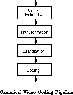
Figure shows a typical video coding pipeline ( e.g.
[JOSV95]). In a conventional FPGA implementation, we
would lay this pipeline out spatially, streaming data through the pipeline.
If we needed the throughput capacity offered by the most heavily pipelined
spatial implementation, that would be the design of choice. However, if we
needed less throughput, the spatially pipelined version would require the
same space while underutilizing the silicon. In this case, a DPGA
implementation could stack the pipeline stages in time. The DPGA can
execute a number of cycles on one pipeline function then switch to another
context and execute a few cycles on the next pipeline function (See
Figure
). In this manner, the lower throughput
requirement could be translated directly into lower device requirements.
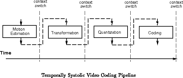
This is a general schema with broad application. The pipeline design style is quite familiar and can be readily adapted for multicontext implementation. The amount of temporal pipelining can be varied as throughput requirements change or technology advances. As silicon feature sizes shrink, primitive device bandwidth increases. Operations with fixed bandwidth requirements can increasingly be compressed into more temporal and less spatial evaluation.
When temporally pipelining functions, the data flowing between functional blocks can be transmitted in time rather than space. This saves routing resources by bringing the functionality to the data rather than routing the data to the required functional block. By packing more functions onto a chip, temporal pipelining can also help avoid component I/O bandwidth bottlenecks between function blocks.
Levelized logic is a CAD technique for automatic temporal pipelining of existing circuit netlists. Bhat refers to this as temporal partitioning in the context of the Dharma architecture [Bha93]. The basic idea is to assign an evaluation context to each gate so that:
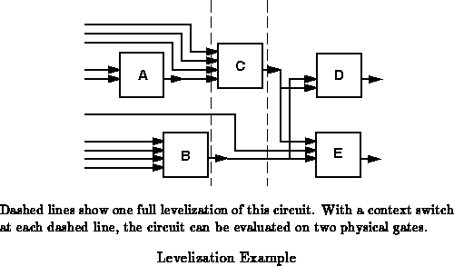
Figure shows a simple netlist with five logic
elements. The critical path (A
C
E) is three
elements long. Spatially implemented, this netlist evaluates a 5 gate
function in 3 cycles using 5 physical gates. In three cycles, these five
gates could have provided
gate evaluations, so we realize
a gate usage efficience,
, of
. The
circuit can be fully levelized in one of two ways:
The preceding example illustrates the kind of options available with levelization.
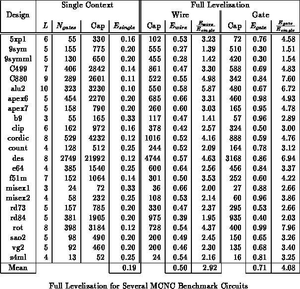
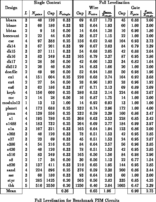
Table summarizes full levelization results for several
MCNC benchmarks. sis [SSL +92] was used for technology
independent optimization. Chortle [Fra92]
[BFRV92] was used to
map the circuits to 4-LUTs. For the purpose of comparison, circuits were
mapped to minimize delay since this generally gave the highest, single
context utilization efficiency. No modifications to the mapping and
netlist generation were made for levelized computation. Gates were
assigned to contexts using a list scheduling heuristic. Levelization
results are not optimal, but demonstrate the basic opportunity for
increased utilization efficiency offered by levelized logic evaluation.
full_wg_expl_long.tex
wire_vs_gate_opt.tex
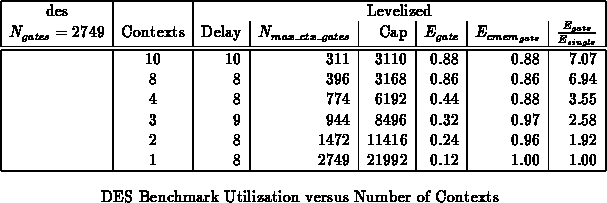
We saw in our simple example above that utilization efficiency varies with
the number of contexts actually used. Table
summarizes the gate efficiencies achieved for the DES benchmark for
various numbers of contexts. The table also summarizes the utilization
efficiency of the context memory (Equation
).
Figure plots both gate and memory utilization
efficiency as a function of the number of contexts.
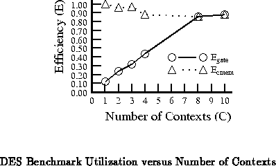
Recall from Section and Figure
that
context memory takes area away from active silicon.
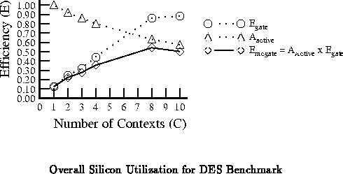
Figure
combines the results from
Table
and Equation
according to Equation
to show the net silicon
utilization efficiency for this design.
In this section we have focussed on cases where the entire circuit design is temporally pipelined. There are, of course, hybrids which involve some element of both spatial and temporal pipelining. An eight level deep piece of logic, for instance,
can be:
In general, once we have determined the level of spatial pipelining necessary to provide the requisite throughput, we are free to temporally pipeline logic evaluation within each spatial pipeline stage.
The performance of a finite state machine is dictated by its latency more than its bandwidth. Since the next state calculation must complete and be fed back to the input of the FSM before the next state behavior can begin, there is no benefit to be gained from spatial pipelining within the FSM logic. Temporal pipelining can be used within the FSM logic to increase gate and wire utilization.
Table summarizes the full levelization of several
MCNC benchmark FSMs in the same style as Table
.
Finite state machines, however, happen to have additional structure over random logic which can be exploited. In particular, one never needs the full FSM logic at any point in time. During any cycle, the logic from only one state is active. In a traditional FPGA, we have to implement all of this logic at once in order to get the full FSM functionality. With multiple contexts, each context need only contain a portion of the state graph. When the state transitions to a state whose logic resides in another context, we can switch contexts making a different portion of the FSM active. National Semiconductor, for example, exploits this feature in their multicontext programmable logic array (PLA), MAPL [Haw91].
In the most extreme case, each FSM state is assigned its own
context. The next state computation simply selects the appropriate next
context in which to operate. Table shows the reduction
in logic depth and increase in utilization efficiency which results from
multiple context implementation. FSMs were mapped using mustang
[DMNSV88]. Logic minimization and LUT mapping were done with
espresso, sis, and Chortle. All single context FSM
implementations use one-hot state encodings since those uniformly offered
the lowest latency and had the lowest capacity requirements. The
multicontext FSM implementations use dense encodings so the state
specification can directly serve as the context select. Delay and capacity
are dictated by the logic required for the largest and slowest state.
Comparing Table to Table
, we
see that this state partitioning achieves higher efficiency gains and
generally lower delays than levelization.
The capacity utilization and delay are often dictated by a few of
the more complex states. It is often possible to reduce the number of
contexts required without increasing the capacity required or increasing
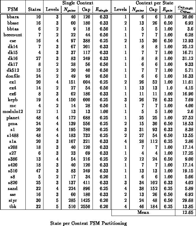
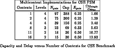
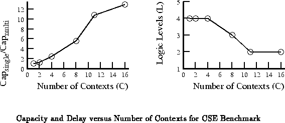
the delay. Table shows the cse benchmark partitioned
into various numbers of contexts. These partitions were obtained by
partitioning along mustang assigned state bits starting with a four
bit state encoding. Figure
plots the capacity and
delay results from Table
versus the number of contexts
employed.
While demonstrated in the contexts of FSMs, the basic technique used here is also fairly general. When we can predict which portions of a netlist or circuit are needed at a given point in time, we can generate a more specialized design which only includes the required logic. The specialized design is often smaller and faster than the fully general design. With a multicontext component, we can use the contexts to hold many specialized variants of a design, selecting them as needed.
Programmable device capacity has both a spatial and a temporal aspect. Traditional FPGAs can only build up functionality in the spatial dimension. These FPGAs can only exploit the temporal aspect of capacity to deliver additional throughput for this spatially realized functionality. As a result, with heavy pipelining, FPGAs can provide very high throughput but only on a limited amount of functionality. In practice, however, we seldom want or need the fully pipelined throughput. Instead, we are often in need of more resources or can benefit from reducing total device count by consolidating more functionality onto fewer devices.
In contrast, DPGAs dedicate some on-chip area to hold multiple configurations. This allows resources such as gates, switches, and wires, to implement different functionality in time. Consequently, DPGAs can exploit both the temporal and the spatial aspects of capacity to provide increased functional capacity.
Fully exploiting the time-space capacity of these multicontext devices introduces new tradeoffs and raises new challenges for design and CAD. This paper reviewed several stylized models for exploiting the time-space capacity of devices. Multifunction devices, segregated utility functions, and temporally systolic pipelining are all design styles where the designer can exploit the fact that the device function can change in time. Levelized logic and FSM partitioning are CAD techniques for automatically exploiting the time-varying functionality of these devices. From the circuit benchmark suite, we see that 3-4x utilization improvements are regularly achievable. The FSM benchmarks show that even greater capacity improvements are possible when design behavior is naturally time varying. Techniques such as these make it moderately easy to exploit the wire and gate capacity improvements enabled by DPGAs.
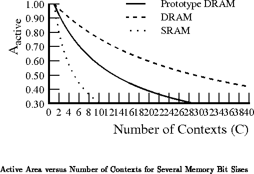
In Section and Figure
we saw how
active capacity varied with the number of supported contexts. In
Section
, we took
technology numbers from the DPGA prototype. The exact shape of the
curves, or more particularly, the
in
Equation
, depends on the memory bit density.
In this section we show this same data for two other, relevant, memory
densities.
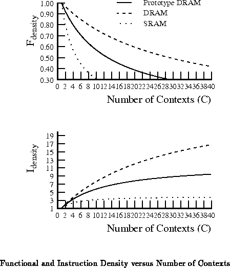
As noted in [TEC +95a], the DPGA prototype used a DRAM cell
with a particularly asymmetric aspect ratio which made it a factor of two
larger than it could have been: 146 vs 75
. Using the tighter
DRAM, we could have placed 8 contexts in the same space as the prototype.
Solving Equation
at this point gives:
.
An SRAM cell would have required 300 per bit instead of
146
. To first order, we could have placed only 2 contexts in the same
space as the prototype context memory. In practice, the SRAM cells would
remove the need for the refresh control circuitry such that the actual area
difference would be smaller than this factor of two implies.
Solving Equation
assuming only two contexts gives
.
Figure plots these three curves together to show
the difference made by these various memory bit densities.
The tradeoff we are making when we add more context memory is to
decrease the density of active computional elements, functional
density, in order to increase the density of diverse operations,
instruction density or functional diversity.
Figure plots both functional
density and the instruction density against the number of contexts for the
memory densities of the previous section.
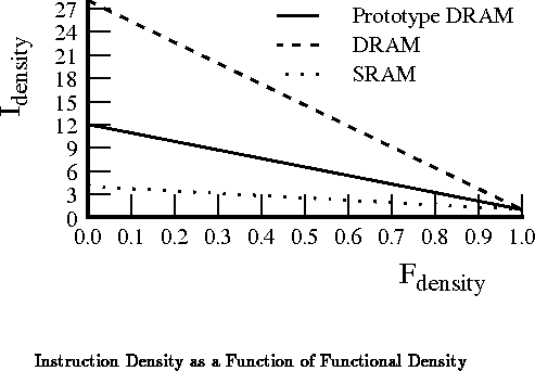
Figure
plots functional density versus
instruction density.
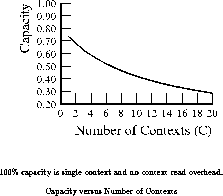
In Section , we also noted that the time taken to read context
memory introduces a delay which increases
, reducing
delivered capacity. Reviewing the DPGA prototype times, without a context
switch
is roughly 7 ns when it includes one LUT evaluation
and one crossbar traversal. The context read adds 2.5 ns to the cycle time.
The result is a 26% capacity loss. Figure
replots
Figure
in terms of capacity to show this effect.
In the DPGA prototype (tn112) (tn114), the only way
to route a signal through a context is via a logic block. The inputs to a
context are limited to the logic and input block flip-flop outputs. In
general, the logic block flip flops are used to communicate results from
one context to the next. As a consequence, if a value produced in context
is consumed at context
and
, a logic block with
associated flip flop must be allocated to route that signal through each of
the intervening contexts (
,
,...,
).
For example, let us reconsider Figure in light
of this restriction. Using the partitioning shown in the figure and
assuming the inputs to the example come from the I/O pins, the middle
stage would require two logic blocks:
With this additional constraint, is is necessary to include the through routing in with the number of gates occupied at a particular level. This produces a different optimization criteria and efficiency metric. During levelization, we are now minimizing the sum of the through connections and gate utilization in the most heavily used context. Efficiency, in this case, is defined as:
Table parallels Table
,
showing the efficiencies achieved under this model. As before, the results
for each circuit shown in Figure
represent a
different levelization than the ones in Table
.
As we expect, the need to dedicate logic blocks for through traffic
decreases the efficiencies achieved.
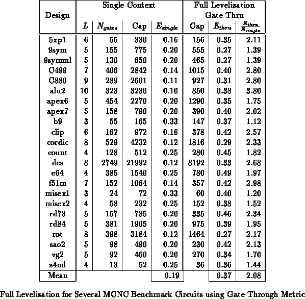
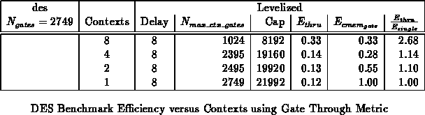
Figure shows the capacity and efficiency for the DES
benchmark as a function of the number of contexts. We see a less graceful
degradation in efficiency under this gate through model.
Under the pure gate and wire models it was theoretically possible to achieve 100% efficiency by adding sufficient levels to balance the contexts. In the extreme, for example, one can evaluate a single gate per context until the entire circuit is evaluated. This is not the case under this model. The through routing only increases as the number of contexts are increased beyond the number of topologically required levels.
Dharma [BCK93] dedicated separate buffer resources for through routing. As a consequence Dharma does not, necessarily, consume gates for through routing. However, this means Dharma has staticly designed in two different kinds of resources for evaluation and made a static partition of interconnect resources between these two functions. Since both approaches have their benefits and drawbacks, it is not immediately clear which is preferable.
It is likely that there is a better alternative than either. For example, it might be worthwhile to create some inter-context ``long lines''. Somewhat like ``long lines'' in conventional FPGAs, these would span multiple contexts rather than spanning multiple rows or columns of array elements. Resources to ``park'' through connections might also be beneficial. Here, we might allocate a place to store and then recover values which are needed at a later time; this is the approach taken in TSFPGA (tn134).
The netlists input to the levelization process were not specifically targeted for levelized computation. Introducing the through routing costs at the network generation level may allow us to produce networks more amenable to efficient levelization.
This is one area which merits attention in the further development of this technology. The combination of the current DPGA routing architecture with the off-the-shelf netlist generation is not extracting as efficient results as appear possible.