Dynamically Programmable Gate Arrays:
A Step Toward Increased Computational Density
Andre DeHon
Original Issue: April, 1996
Last Updated: Mon Jul 8 11:39:35 EDT 1996

``How big is a computation?''
The design goal for ``general-purpose'' computing devices is to develop a device which can:
We know, for example, that a four input Lookup Table (4-LUT)
occupies roughly 640K ( e.g. 0.16mm
in a 1
CMOS
processor (
)) [CSA +91] [TEC +95].
Thus, we get a 4-LUT density of 1.6 4-LUTs per one million
of
area.
At the same time, we notice that the descriptive density of 4-LUT designs can be much greater than the 4-LUT density just observed. That is, the LUT configuration is small compared to the network area so that an idle LUT can occupy much less space than an active one.
For illustrative purposes, let us assume that it takes 200 bits to
describe the configuration for one 4-LUT, which is typical of commercial
FPGA devices. A 64Mb DRAM would hold 335K such configurations. Since a
typical 64Mb DRAM is 6G, we can pack 56 4-LUT descriptions per
one million
of area -- or about 35
the density which we
can pack 4-LUTs. In fact, there is good reason to believe that we can use
much less than 200 bits to describe each 4-LUT computation
[DeH96b], making even greater densities achievable in
practice.
Returning to our original question, we see that there are two components which combine to define the requisite area for our general-purpose device:
In an ideal packing, a computation requiring active
compute elements and
total 4-LUTs, can be implemented in area:
In practice, a perfect packing is difficult to achieve due to connectivity
and dependency requirements such that configuration
memories are required.
When , it is advantageous to associate multiple, ideally
, LUT descriptions with each active LUT.
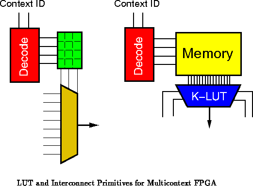
Dynamically Programmable Gate Arrays (DPGAs), do just that, packing several
configuration memories for each active LUT and switching element
(Figure
).
From our own experience with the DPGA [TEC +95]:
The base LUT area is generally consistent with other FPGA implementations.
Our
is based on a DRAM cell design which is
600
per memory bit, making the memory cells 2
smaller
than an SRAM implementation. A static memory would be closer approximated
as:
An aggressive DRAM cell should realize a 300
memory cell,
making:
In all these cases the configuration size is at least an order of
magnitude smaller than the active LUT:
Single context devices running designs where the descriptive
complexity, , is large compared to the number of requisite parallel
operations,
, are, consequently, much larger than they need to be
since they require
more active LUTs than are necessary to
support the task at the desired computational speed.
Of course, there are many issues and details associated with
multicontext computing devices. In this section, we will walk through a
specific design example in order to make the previous discussion more
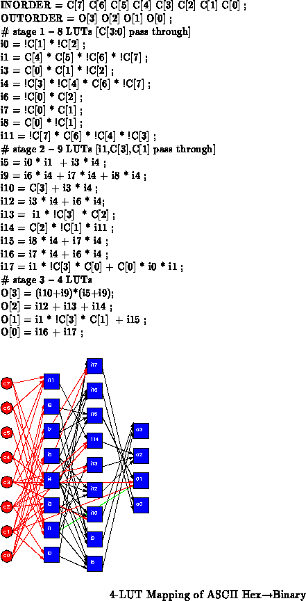
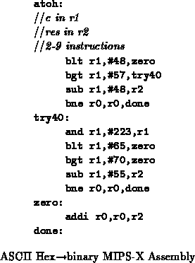
concrete and in order to motivate additional issues. We will take an ASCII
Hexbinary converter as our example.
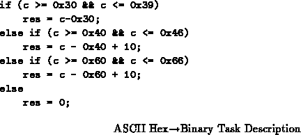
Figure describes the basic conversion task. Assuming we care
about the latency of this operation, a mapping which minimizes the critical
path length using SIS [SSL +92] and Chortle [Fra92] has
a path length of 3 and requires 21 4-LUTs. Figure
shows the LUT mapping both in equations and circuit topology.
The multicontext implementation requires:
In contrast, a non-pipelined, single-context implementation would require
LUTs, for an area of:
If we assume that we can pipeline the configuration read, the multicontext device can achieve comparable delay per LUT evaluation to the single context device. The total latency then is 21 ns, as before. The throughput at the 7 ns clock rate is 48 MHz. If we do not pipeline the configuration read, as was the case for the DPGA prototype [TEC +95], the configuration read adds another 2.5 ns to the LUT delay, making for a total latency of 28.5 ns and a throughput of 35 MHz.
If the 35-48 MHz implementations are still faster than required by
the application, we can reduce even further. Ideally,
if we did not have to worry about retiming issues:
That is, if we can afford
LUT
delays, and we can evaluate
LUTs per cycle, we only need enough
active LUTs such that
. E.g. if we
required less than 4 MHz operation, we should need only one active LUT.
In practice, as long as we have to retime intermediates through
LUTs as noted above, there will be a limit to our ability to reduce the
maximum stage size by adding temporal pipeline stages.
Even if we only had to arrange for the four LUT inputs needed for a
single LUT evaluation in stage , we would have to deploy at least 4 LUTs
in stage
to carry the signals needed by that single LUT in stage
.
If the only place where intermediate signals can exist is on LUT
outputs, as assumed so far, we eventually reach a lower limit on our
ability to serialize active resource usage -- decreasing active resource
requirements by reusing them to evaluate different LUTs in sequence. The
limit arises from signal connectivity requirements. For the ASCII
Hex
binary mapping considered above, the 3 cycle,
case is the effective limit.
To achieve further reductions it is necessary to relax the
restriction that all inputs to an evaluation stage be delivered from
active LUT outputs from the immediately prior evaluation stage. One way to
achieve this is to associate a pool of memory with each active LUT. This
pool serves the same role as a register file in a traditional processor.
VEGA [JL95] uses this approach achieving:
Where:
when:

A similar alternative is to move the flip-flop which normally lives
at the output of a LUT to its inputs and to replicate this for each
described LUT rather than only associating such flip-flops with active
LUTs. Figure contrasts this scheme with the
scheme used in the original DPGA prototype and with traditional LUT
organizations. The basic idea is to latch each LUT input on the cycle
which it is produced even when the LUT will not be evaluated on immediately
subsequent cycle. Figure
elaborates upon this
configuration. Since each virtual LUT in a group shares each input line,
it is not possible to load two different signals into the same input
location of different LUTs on the same cycle. Also, since all the inputs
to a virtual LUT are latched, the LUT output can be produced on multiple
cycles if routing restrictions such as these require it to be generated
multiple times.

Adding these matching units and input flip-flops will, of course, make
the described contexts larger.
From our own experience, we estimate:
Together, this gives us:
In the most extreme serial case, ,
. This
implementation requires area:
Running at a 9.5 ns LUT cycle, this implementation has a 200 ns latency
achieving 5 MHz operation.
Excessive serialization is expensive since we need to add resources
to hold intermediate values. Another way to share resources while meeting
a lower computational rate is to overlay multiple, independent computations
into the same space. This allows each computation to have wide stages as
in Section , while still taking advantage of low
throughput requirements.
In our example above, we might run 12 LUTs on the same 21 cycle round
to achieve 5 MHz throughput for the ASCII conversion. The conversion
itself only occupies these 28 LUTs for 3 cycles, leaving 18 cycles during
which the array can be used for other tasks. Array costs are now in line
with Equation . The amortized cost for this implementation
is then:
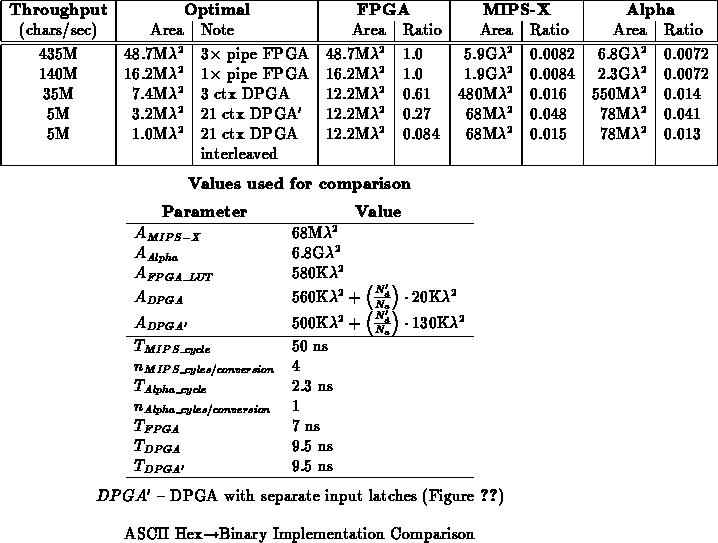
Table summarizes the area for various implementation points
described in this section. Also included is the effective area required
for two different processor implementations of this task. The MIPS-X
[HHC +87] assembly code is shown in Figure
; for
the sake of comparison, we assume the 4 cycle path which occurs when
converting an ASCII decimal digit. The DEC Alpha [GBB +96]
implementation assumes that the conversion is performed by table lookup and
the table is already loaded into the on-chip data cache; the conversion
takes one add and one lookup, each of which take up half a cycle since the
Alpha can issue two instruction per cycle. The processor area comes from
scaling the actual area to meet the cycle time -- this assumes that we
either deploy multiple processors to achieve a higher rate of execution
than the base processor cycle time or that the task shares the processor
with other tasks and area is amortized accordingly.
In this section, we have examined one task in depth. See [DeH96a] for a broader look at multicontext applications.
One thing which is clear from Table is that there is
an optimal ratio between
and
which varies with the desired
throughput requirements. Unfortunately, we cannot expect to have a distinct
DPGA design for every possible number of contexts.
We can define a throughput ratio as the ratio of the desired task throughput to the raw LUT throughput:
Here, we have been assuming MHz for conventional
devices. When
, single contexts are very inefficient since far more
active LUTs are provided than necessary. When
, where
is the
number of contexts supported, area is unnecessarily consumed by context
memory. Figure
plots
versus
showing the relative
efficiency of running a task with throughput ratio
on a device with
contexts for both the DPGA context sizes and DPGA
sizes.
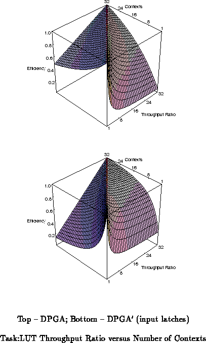
One interesting design point to notice on both graphs is that point
where the area dedicated to the fixed LUT is equal to the area of the
contexts. This occurs at for the DPGA and
for DPGAs with
input latches. At this point, the efficiency never drops below 50% for
any values of
. This is interesting since the cross efficiencies at the
extremes in the graph shown drop down to 13%.
In a quick review of the FPD'95 proceedings, we see
FPGA task implementations running at frequencies between 6MHz and 80MHz,
with most running between 10MHz and 20MHz. Thus, we see a decent number of
FPGA tasks implemented with . We might ask why these applications
have such large throughput ratios,
. There are two main causes:
Multicontext FPGAs have the potential to pack typical computational tasks into less area, delivering more computation per unit area -- i.e. increased computational density. The key properties they exploit are:
Task dataflow dependencies require that a number of signals be made available to each stage of computation. The retiming requirements associated with satisfying these dependencies can pose a limit to the effective serializability of the task. In some cases we can avoid these limitations by overlaying loosely or unrelated tasks on the same resources. Alternately, we can architect intermediate data storage to allow serialization, at the cost of larger context resources. Architectural design of these multicontext structures and synthesis for them is a moderately young area of research. Interesting research possibilities exist in the areas of:
Jeremy Brown, Derrick Chen, Ian Eslick, Ethan Mirsky, and Edward Tau made the DPGA prototype possible. The input latch ideas come from the TSFPGA architecture co-developed with Derrick Chen. Many of the quantitative details about the DPGA are the results of the collected efforts of this team.