Stack Packaging Technology
Fred Drenckhahn
Tom Knight
Andre DeHon
Original Issue: December 1990
Last Updated: Mon Nov 8 17:13:10 EST 1993

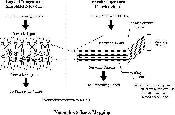
We have developed a novel scheme for three-dimensional packaging of components. Our packaging scheme sandwiches layers of components between conventional printed circuit boards to achieve a stacked component structure. Custom connectors built around button balls along with custom component packages are utilized to achieve the vertical interconnect in our system. In this paper, we describe our packaging scheme focusing on the constituent components and system issues including controlled impedance traces, high-speed signalling, cooling, and system repair. We show how our stack packaging scheme can be used to efficiently package a multistage interconnection network.
< insert general description of stack structure >
< insert description of our dual-sided pad grid array >
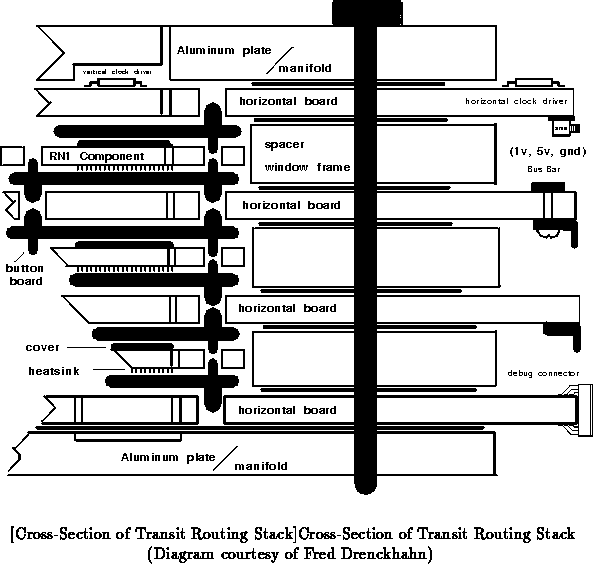
< insert description of our button boards >
< insert description of PC board technology used >
< describe cooling strategy >
< describe controlled impedance traces (stripline sturcture), button board connections, large proportion of power pins on chip, capacitors on compoment, etc. >
< solderless connections -> trivial replacement >
< mapping network onto stack, routing compoment packaged in dspga372, etc. >