Unifying FPGAs and SIMD Arrays
Michael Bolotski, Andre DeHon, and Thomas F. Knight, Jr.
Original Issue: September, 1993
Last Updated: Tue Mar 8 15:43:06 EST 1994

Field-Programmable Gate Arrays (FPGAs) and Single-Instruction Multiple-Data (SIMD) processing arrays share many architectural features. In both architectures, an array of simple, fine-grained logic elements is employed to provide high-speed, customizable, bit-wise computation. In this paper, we present a unified computational array model which encompasses both FPGAs and SIMD arrays. Within this framework, we examine the differences and similarities between these array structures and touch upon techniques and lessons which can be transfered between the architectures. The unified model also exposes promising prospects for hybrid array architectures. We introduce the Dynamically Programmable Gate Array (DPGA) which combines the best features from FPGAs and SIMD arrays into a single array architecture.
FPGA-based custom computing engines and massively parallel SIMD arrays [BRV93][Bol93][Gea91] have been demonstrated to provide supercomputer-class performance on some tasks at a tiny fraction of supercomputer cost. Both of these architectures consist of arrays of small yet numerous processing elements. This similarity is the key to understanding their surprisingly high performance: most of the silicon in the FPGA and SIMD chips is actively operating on data bits. SIMD machines achieve high utilization by massive data parallelism. FPGA machines achieve high utilization by task-specific hardware configuration and pipelining. In both cases, several thousand bits are transformed per cycle, compared to the 64 bits of a typical microprocessor. In this paper we show that the similarities extend considerably further, and indeed that the two architectures can be viewed under a common computing model.
Field-Programmable Gate Arrays (FPGAs) are widely used today to implement general-purpose logic. FPGAs are built from a moderately fine-grained array of simple logic functions. An FPGA array is customized by selecting the logical function which each array element (AE) performs and the interconnection pattern between AEs. Using multiple stages of logic and primitive state elements, these arrays are programmed to implement both sequential and combinational general-purpose logic. FPGAs are in wide use today for system customization and glue logic, low-volume application-specific designs, and IC prototyping. A variety of FPGAs are commercially available from a number of vendors ( e.g. Xilinx [Inc91], Actel [Act90], Atmel [Fur93], Lattice [Qui92]).
Single-Instruction Multiple-Data (SIMD) arrays are employed to realize high throughput on many regular, computationally intensive data processing applications. An array of simple, fine-grained computational units make up most SIMD arrays. Typically, the computational units are wired together through local, nearest-neighbor communications. On each clock cycle, an instruction is broadcast to all AEs, and each AE performs the indicated computation on its local data element. SIMD arrays are commonly used for algorithms requiring regular, data-parallel computations where identical operations must be performed on a large set of data. Typical applications for SIMD arrays include low-level vision and image processing, discrete particle simulation, database searches, and genetic sequence matching. NASA's MPP [Pot85], Thinking Machines' CM-2 [Hil85], and MasPar's MP-1 [Bla90] are early examples of large-scale SIMD arrays. Increased silicon area along with advanced packaging trends allow production of very high-performance, highly-integrated, SIMD arrays at reasonable costs [BBLC93], [Lea91].
Viewed at an abstract level, these two array architectures are very similar. Both employ a moderately fine-grained array of logic elements. Each logic element performs a simple logic function on some state and some inputs from the array and either updates its own state to record the results of its computation or shares the results with other elements in the array. Despite the similarity, the design of FPGAs and SIMD arrays has evolved along quite divergent paths.
In this paper, we introduce a computational array model encompassing both FPGAs and SIMD arrays. By highlighting the tradeoffs made in the model to arrive at FPGA or SIMD structures, we can better appreciate optimizations made in the engineering of high-performance computational arrays. Further, we can transfer lessons learned between various array architectures. Additionally, the unified model highlights potentially novel hybrid array architectures. We examine one such hybrid, the Dynamically Programmable Gate Array (DPGA), and show that it can subsume the role of traditional FPGAs or SIMD arrays.
In Section we introduce the uniform computational array model and show
how FPGAs and SIMD arrays relate to this model. In Section
we
compare the manner in which FPGA and SIMD arrays solve problems by
considering the mapping of computations from one architecture to the other.
In Section
we introduce the DPGA hybrid architecture and describe its
benefits and costs. In Sections
through
, we
examine these arrays at a somewhat abstract level, ignoring for the most
part, technology-specific optimizations during implementation. In
Section
we discuss the ways in which computational arrays are
optimized based on computing style and available technology. In
Section
we review the key themes explored in this paper.
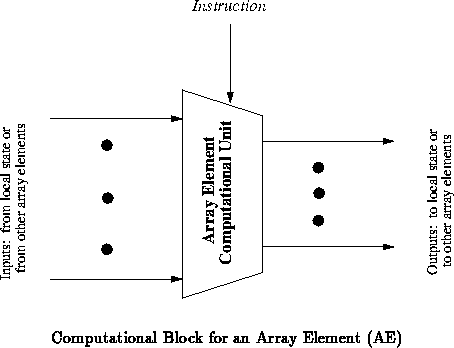
A computational array is composed from a regular lattice of AEs along with
interconnection resources linking AEs together. Abstractly, each AE
performs a simple computation on its inputs to produce one or more output
bits (See Figure ). The inputs come from local state or via
communication channels from other AEs. The outputs are either stored to
local state or are communicated to other AEs. An instruction is used
to specify the computation performed by each AE. Instructions are
typically also used to specify communication and state manipulation,
although in this paper we focus primarily on the instruction as
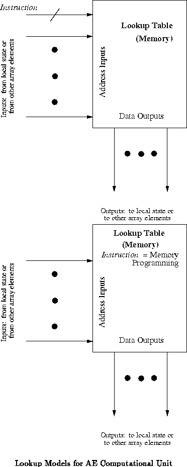
specifying the operation of the logic unit. In this simplified model, the
transform from input values to outputs is modeled as a lookup table
addressed by the input value (See Figure
). We can model the
instruction as either the programming of the lookup table or as
additional inputs to the lookup table (See Figure
).
In the most general setting, we might wish to specify a
different instruction for each AE on each computational cycle.
Unfortunately, if we design such an array, the resources required
for instruction distribution dominate the array geometry and the
required instruction bandwidth is unmanageably large. In practice, the
manageable instruction bandwidth limits the operation rate of
the array. With a -element array where each
element implements
distinct functions,
Equation
shows the relation between computational
cycle time,
, and instruction bandwidth,
.
For example, a 100 element array with 64-function elements operating at
10 MHz, requires /100 ns = 6 Gbits/sec. If we are limited
to an instruction distribution bandwidth of 1 Gbit/s, the clock cycle for
the array must be limited to
/
= 600 ns.
FPGAs and SIMD arrays both weaken this general computational model to avoid the requirement for huge instruction bandwidth. By simplifying the model, each type of array achieves a more pragmatic balance of resource requirements. For certain classes of applications these simplified models are adequate and can be engineered to take full advantage of the implementation technologies available.
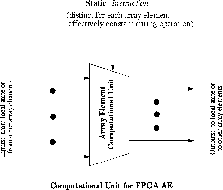
FPGAs weaken the model by eliminating the instruction (See
Figure ) and therefore not changing each AE's operation
through time. Different AEs, however, can be executing different operations.
During a slow programming phase, each AE is configured with its
operation, which remain fixed during subsequent normal operation. In
SRAM-programmable FPGAs ( e.g. Xilinx LCA [Inc91], Atmel
[Fur93]) this programming phase normally occurs once each time the
system is powered on. In fuse or anti-fuse based FPGAs ( e.g. Actel
[Act90] ) a device is
programmed exactly once during its lifetime.
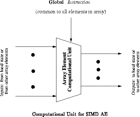
SIMD arrays weaken the model by distributing the same instruction to
every AE (See Figure ). Each AE is allowed to perform a
different operation on each computational cycle, but all the elements in
the array are required to perform the same operation during any given
cycle.
These two compromises weaken the model along orthogonal dimensions. FPGAs compromise in the rate of instruction dispatch to allow the instructions to vary spatially through the array. SIMD arrays compromise in the spatial variation of instructions to allow a high rate of instruction dispatch.
We can view the compromises made in arriving at FPGA or SIMD arrays as space-time tradeoffs. FPGAs allow us to spatially construct any logical operation by composing an ensemble of AEs which implements the operation spatially. SIMD arrays allow us to temporally perform any logical operation by sequencing through the operations required to perform the operation in time. We can see this tradeoff further by considering how we can naively map an arbitrary FPGA computation onto a SIMD array and vice-versa.
Since we can wire any sequential or combinational logic function on an FPGA array, we can simulate a SIMD AE by wiring up a group of FPGA AEs. Further, we can compose FPGA-implemented, SIMD AEs to simulate an arbitrary SIMD array. We can then run the same SIMD computation which we would have run on the SIMD array on the FPGA implementation.
Indeed, if the routing resources required to broadcast the same instruction to every simulated SIMD AE are directly available in the FPGA architecture, the implementation is extremely simple. In traditional SRAM-based FPGAs, one cell can serve as the SIMD AE computational element, one can serve as the local memory, and two can serve as the configurable interconnect.
We can simulate any non-asynchronous FPGA in time using a SIMD array. To
do so, we note that most SIMD arrays provide a bit mask to
disable a subset of the cells for a particular operation.
Conceptually, we map each FPGA AE to a corresponding SIMD AE. For each
FPGA gate delay, we dispatch instructions, one for each different
instruction the FPGA AE can perform. If necessary, we then dispatch a
series of instructions to route output bits from producers to consumers.
With each dispatch, the SIMD AEs are masked such that the only elements
which perform a given operation are those which correspond to FPGA AEs
which are programmed to perform the given operation.
The FPGA implements the SIMD array spatially, and simulation overhead appears as a requirement for more gates and wiring resources. The SIMD array implements the FPGA temporally, and simulation overhead slows the computation rate. Of course, simulation is not the best approach for porting an algorithm from one architecture to the other. Nonetheless, the constructions above establish the feasibility of translating arbitrary computations between the two kinds of arrays.
In this section we introduce a hybrid architecture which allows instructions to vary both spatially and temporally without requiring additional instruction bandwidth.
As we saw in Figure , the lookup table modeling each
SIMD, computational AE is programmed identically on all AEs in the array.
In Figure
we saw that each FPGA AE lookup table is
programmed differently to select a different instruction on each AE. In a
Dynamically Programmable Gate Array (DPGA) we allow the lookup table
in each AE to be programmed differently. This allows each AE to perform a
different operation in response to each broadcast instruction
(See Figure
).
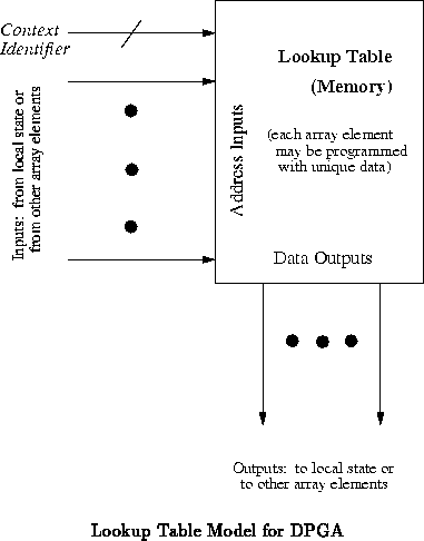
Figure shows one way to view the DPGA AE. We think of
the broadcast instruction as a context identifier (CID). The
local instruction store in each computational element selects the
executed instruction by table lookup using the CID as an address. Each
AE holds a distinct instruction store, and hence different AEs execute
distinct operations at the same time.
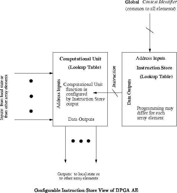
We can also think of the DPGA as an FPGA with multiple contexts. All the instructions programmed into a particular CID location in the AE's instruction stores can be thought of as one array-wide configuration. When we change the CID, we change contexts and instantly reconfigure the entire array.
In Figures
and
, we only show how the CID selects the
operation performed by the computational unit of each AE. In practice, the
routing resources interconnecting AEs and the addresses of local stored
data are also configured by the instructions. The CID must select the
instructions which configure the interconnection and addressing as well as
the computation.
The DPGA retains all the facilities of both FPGA and SIMD arrays. If we wish to perform traditional SIMD operations, we simply program the same instructions into all the instruction stores. If we wish to perform traditional FPGA operations, we continually broadcast the same CID.
For maximum flexibility, the DPGA instruction data is writable by some combination of the instruction stream and local AE state. This allows the array to rapidly update context programming as necessary. If we think of the instruction store as a context cache, the writable instruction store allows high speed cache replacement. In cases where the sequence of distinct instructions is larger than the instruction store, we include code in the instruction stream to reload the instruction store.
This hybrid architecture increases flexibility for both implementation and application of computational arrays. We can immediately identify several benefits which the DPGA architecture has over either SIMD arrays or FPGAs.
The width of the CID field is unrelated to length of the stored instruction, but is typically much shorter. Since instruction distribution bandwidth is a major design constraint in high performance SIMD arrays, this reduction can be very important. For example, a complex FPGA cell might provide five input logic functions. Distributing a truth table for such a function requires 32 instruction bits; a CID as small as 8 bits might suffice for most applications, reducing the required instruction bandwidth by a factor of four.
A single DPGA array type can be engineered and produced to satisfy applications which have traditionally been served by either FPGAs or SIMD arrays. By combining the market base of these two array types, DPGAs can become commodity products, allowing cost effective implementation of novel data-parallel processors as well as more effective replacements for FPGA structures.
Viewing the DPGA from a traditional SIMD view, we have added the ability to simultaneously perform different operations. This is useful in cases where the pieces of the data in the array must be operated on differently or there is insufficient data parallelism to occupy the entire array performing the same computation on an operation cycle.
Boundary conditions are a common case where non-uniform data handling is required. In the DPGA model, boundary cells are programmed to perform a different set of operations from interior array cells during some computation. One particularly compelling example of such boundary processing is the use of a DPGA array for bit-parallel arithmetic operations, where the most- and least- significant bits of each parallel data word usually require special handling.
Viewing the DPGA as a traditional FPGA, we have added a configuration cache
and the ability to perform zero-latency reconfiguration between cached
configurations. With the hybrid configuration, we can perform computations
in time-slices and achieve much more efficient utilization of AEs. In
conventional FPGAs, most AEs are exercised at their full operational speed
for only a small portion of the clock cycle. That is, each AE is part of
some path between sequential elements which are clocked at the component's
system clock rate.
Assuming there are AEs in the critical path between
sequential elements for a computation and each AE can operate in time
, the system clock cycles is at least
. A
given AE only performs its function during
of the cycle and
spends the rest of the time holding its value. By pipelining and
time-slicing the computation, we can arrange for each AE to perform its
computation at the correct time to produce the desired result without
increasing the overall latency of computation. Each of the AEs is now
available on the remaining
time slices to
perform other operations. Consequently, we can schedule other operations
on each AE during these unused cycles. We can effectively interleave
computations and thereby extract higher throughput from an array of a given
size.
In practice, each pipeline register introduces some timing overhead.
If we call the overhead of the pipeline register due to setup and
hold times on the register, then the entire computation would really
require
. If
, then the
overhead is small and often worth paying to increase throughput. If
is larger, it often still makes sense to pipeline but at a larger
granularity. In general, we can divide the
-element critical path into
-element segments and only place pipeline boundaries
between the segments. Here we slow the computation down as shown in
Equation
.
At the same time, we allow an additional throughput as shown in
Equation .
Of course, traditional FPGAs can use their own registers to pipeline computations and increase throughput. The multiple loaded contexts allow each DPGA AE to be reused to perform different functions during each time slice.
In analogy to the Virtual Processor concept used in the SIMD Connection Machine [Hil85] to map a large computation onto a small number of processors, we can also treat the DPGA as having many Virtual Cells per physical AE. At a given point in time one function is active at each AE. Using the CID, we can switch the personality of each AE amongst the virtual cells it is emulating. This allows a small DPGA array to efficiently emulate a larger FPGA array.
The virtual cells approach can also be viewed as a technique for reducing the system part count. Rather than collect enough FPGA components to spatially implement all the functions required at any point in time, we employ a single DPGA with an external memory or ROM chip to store additional contexts. A controller inside the DPGA sequences through contexts, swapping them from external memory when necessary. The DPGA can then switch between configurations sequentially to perform the complete ensemble of required functions.
The logical extension of this integration process is to implement the DPGA in a high-density DRAM process and therefore integrate the programmable logic with a memory store. The combined chip is able to perform almost any logic operation, with a slowdown increasing with operation complexity.
FPGAs are in common use today for logic emulation. Most emulation systems directly map gates in the emulated system to gates in the FPGA. This uses the FPGA AEs inefficiently for the reasons identified above. The hybrid AEs can be used more efficiently by scheduling multiple gates in the emulated system to a single gate on the FPGA and using time-slice computation as above. The CID also provides the opportunity to perform Event-Driven Simulation. Like software oriented event-driven simulation, we can take advantage of the fact that some subsets of the system change infrequently. Using the virtual cells model, we can ``swap'' in a region of logic and emulate the region only when its value changes.
From both the FPGA and SIMD array standpoint, the primary additional cost
for the DPGA array is the area for the instruction store lookup table (See
Figure ). The instruction store can be implemented with a
single-port, SRAM-style memory array which can be implemented very
compactly in a full-custom design.
For example, 70% of each Abacus AE [Bol93] comprises roughly 80
bits of SRAM memory. The Abacus AE requires 16 instruction bits to specify
the operation performed by the ALU on each cycle. We could add another
80-bit SRAM to serve as a 5-entry context cache. If we distribute a fully
decoded CID to avoid the area overhead of a decoder at each instruction
store, we reduce the instruction distribution bandwidth from 16 bits per
cycle to 5 bits per cycle while increasing the AE cell area by 70%.
The area cost may not even be an issue if the number of AEs on a chip is
limited by the number of pins available.
Indirection through the instruction store lookup array need not impact the AE cycle time. We can add a pipeline register between the program store output and the array computational element. This pipelining allows the array computational element to run just as fast as it did in the SIMD or FPGA array. The addition of a pipeline stage adds another latency stage to instruction distribution. This has no net loss when compared to the FPGA case where no instruction distribution occurs. The additional cycle of latency due to this pipeline stage is small compared to the typical latency in the instruction distribution path for a SIMD array. In a modern high-speed (> 100 MHz) SIMD array, there are at least three pipeline stages in the instruction delivery phase. Further, there are at least three stages in the return conditional information path. For efficient operation, SIMD arrays generally run long instruction sequences without interruption so that pipeline depth is not a significant issue.
The need for local configuration in SIMD arrays is demonstrated in part by some small steps which SIMD architectures have taken towards local configuration. Several architectures allow local state bits to modify the transmitted instruction, the transmitted address, or the local network connections. This local modification is referred to as operational, address, and connection autonomy where autonomy indicates that processors have the ability to not perform identical operations [ML89]. The translation process is typically very simple: operational autonomy is achieved by potentially inverting the ALU output; addressing autonomy by modifying a few low order bits of the address [BDHR88]; connection autonomy by configuring a network crossbar at each AE site [ML89].
All of these techniques can be viewed as resource-limited implementations of the DPGA architecture. Each can be derived by starting with a small number of contexts and observing that the instructions in each context are almost identical except for a few bits. Factoring out the common bits in hardware leads immediately to the ad hoc implementations described above. Thus, the DPGA model subsumes the local configuration mechanisms in SIMD machines.
In this section we show that the different computing styles used by the FPGA and SIMD architectures drive important architectural trade-offs. We also show that these trade-offs have led to architectural extremes which are often not optimal given available technologies. We show examples where improvements result when we match architecture to the available technology. In many cases, technology-oriented optimizations move us away from the architectural extremes, increasing the similarity between the resulting SIMD and FPGA arrays.
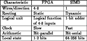
Most implementations of the two architectures compute in two distinct styles: FPGAs unroll their computations in space, while SIMD machines unroll their computation in time. This unrolling can be described as bit-parallel and bit-serial computations, respectively. Bit-serial techniques exhibit comparatively high latency, but are very efficient in terms of throughput and silicon area; bit-parallel techniques produce results quickly but require considerable silicon and routing resources. Because most FPGAs were used to construct controller circuits in which the operation latency was crucial, they were optimized for bit-parallel operation. SIMD AEs were optimized for high throughput, and therefore for bit-serial operation. Upon examination of the two computing styles, the architectural differences required to support them become obvious. The three key areas for comparison are interconnect resources, local state, and clocking strategy.
Bit-parallel operation requires significant interconnection resources to compose complex logical functions of simultaneously existing bits, and the the interconnect pattern need not change through time. Local state is largely unnecessary since intermediate result bits are stored on the wires. Comparatively slow clocking is required to allow computation to ripple through several combinational units in a single cycle.
Bit-serial operation has the opposite requirements. Only a simple logical function, usually on the order of a one-bit adder, need be performed at each step. Some local state is required to store the intermediate results. Little wiring is required since the composition occurs in time, not in space. In some sense, memory cells replace the wires of a bit-parallel design for both storage and communication. Finally, fast clocking is desirable since many simple steps are required for any significant computation.
It is instructive to note that when an implementation of each architecture adopts the opposite computing style, it begins to resemble the opposite architecture. For example, the Abacus machine, a SIMD architecture designed for bit-parallel operation, has a four-input/two-output logical unit, two wires, and only 64 state bits in each AE [Bol93]. In the opposite direction, the Concurrent Logic FPGA AE, targeted specifically for computing rather than implementing random logic, has reduced routing resources, a simple logical unit, and is intended to be clocked at high rates [Fur93].
In the remainder of this section, we discuss these three differences in further detail. We note how the available technology influences implementations. In many cases, technology encourages implementations of these arrays which are not as disparate as the architectural ideals.
The main difference in interconnection between the SIMD and FPGA architectures is that the first dynamically routes multiple logical signals over a single wire, while the second statically assigns a dedicated wire to each signal. In the following two examples, the adoption of the opposite communication style has improved performance.
Static routing, as practiced in the SIMD community, may well be applicable to better utilization of internal routing resources. Chip area allocated to programmable interconnect may be reduced if the wires can be used more efficiently by high-speed, time-multiplexed operation.
Multiple wires are possible in many SIMD implementations because local routing channels to route additional signals between AEs take up little or no additional area in the SIMD array. The additional channels can be used to increase the communication bandwidth between AEs and therefore increase computational efficiency.
Specifically, multiple wires reduce the overhead of dynamically reconfiguring the SIMD network. For example, in a bit-parallel computation the result of a data word comparison must be broadcast to each AE operating on a bit of the data word, so that the entire group can be disabled or enabled as a unit. But in a magnitude comparison, the result bits travel from LSB to MSB. Upon completion, the bit stored in the MSB must be broadcast, which involves turning the network around. This turning around step can take almost as long as the actual comparison. With two network wires, the overhead is eliminated completely.
Modern SIMD architectures are designed with a very high clock rate to compensate for the simple logic operation in each cycle. In contrast, FPGA arrays are clocked comparatively slowly, to allow propagation through several stages of combinational elements. We now describe why FPGA arrays should be clocked much faster than SIMD arrays.
In the current technology trend, on-chip clock speed is increasing much faster than off-chip communication bandwidth. This presents a problem for SIMD arrays. For example, the internal cycle time of a SIMD AE implemented in a 0.8 micron CMOS process can be as low as 5 nanoseconds. Delivery of a wide, 50-bit instruction at 200 MHz to each SIMD chip is a challenging design problem. We see that the factor limiting cycle time is the instruction bandwidth and that ultimately, SIMD AE complexity will have to increase in order to match internal cycle time to available bandwidth.
FPGA architectures do not suffer from these bandwidth limitations since they do not require instructions, and can therefore only benefit from switching to high-speed clocked, pipelined operation. External system design complexity need not increase, as the fast clock can remain purely internal, with chip interfaces operating at low speed. The fast internal clock can be generated with a phase-locked loop from a slow external clock [HCC +93]. Also, a clocked system allows the use of low-power, clocked logic families such as dynamic logic.
As discussed earlier, SIMD machines require considerable local state to store intermediate results, while FPGAs store these results on the wires connecting combinational blocks. The problem with a large amount of state is the need to address it. For example, most SIMD AEs have at least 64 local state bits, requiring 6 bits to specify each read and write address. This is significantly more bits than the 8 required to fully specify a 3-input ALU operation. Clearly, the need to address local state can dominate the instruction bandwidth requirements of SIMD architectures.
FPGA AEs do not have this problem, as their local state typically consists of a single register, which is addressed implicitly by connecting it to the logical unit. In practice, some FPGA cells can be used as a small memory, but we do not consider this part of an AE, as many AEs must be connected together to implement an address generator.
This dissimilarity is another aspect of the static versus dynamic allocation encountered in the interconnect control. When FPGAs need to access a state bit, they statically allocate a wire from the memory cell to the appropriate logic block; SIMD machines must pay the overhead of dynamic access on every cycle, even if the same address is being used for many cycles in a row. Once this observation is made, several techniques for reducing the overhead of dynamic addressing can be evaluated with respect to a particular technology. These techniques include implicitly addressed accumulators, register windows, and register renaming.
Starting from a common computational array model, we examined the similarities and differences between FPGA and SIMD arrays. While both are composed from arrays of fine-grained computational elements, they differ substantially in how they compute. SIMD arrays are employed for high-throughput computations using bit-serial computing techniques. To match this function, SIMD arrays are optimized to vary computation in time while performing the same operation on all array elements at each time step. FPGAs are employed for low-latency computation using bit parallel computing techniques. Optimized for bit-parallel computations, FPGAs are configured statically, and perform computation spatially.
We introduced a hybrid computational array architecture, the DPGA, and showed that it can provide better performance than either. The DPGA allows computation to vary both spatially and temporally. Using a local instruction store, the DPGA performs spatially varying computation requiring no additional bandwidth. The DPGA mixes both bit-parallel and bit-serial computations in a single array structure. We suggested examples where this additional flexibility allows higher performance or lower part count than pure FPGA or SIMD alternatives.
Finally, we explored the influence of bit-serial and bit-parallel computing styles on the details of array implementation. We saw that these two computing paradigms push array organization towards opposite extremes of clocking, routing, and state management. We further saw that these extremes are often less than optimal when one considers the technology available for array implementation. Hybrid approaches often extract the highest performance in a given technology. Based on these observations, we believe there is room for significant cross-fertilization of ideas between the FPGA and SIMD communities.