Previous: Structure and Composition of Reconfigurable Computing Devices Up: Structure and Composition of Reconfigurable Computing Devices Next: Instructions
Programmable interconnect is the dominant contributor to die area and cycle time in configurable devices. To support their large, active functional density, the computational units must be richly interconnected and support highly parallel data routing. FPGAs, more than other general-purpose devices, place most of their area into interconnect.
We review interconnect issues in the context of on-chip networks for
reconfigurable architectures. We establish typical size and delay
contributions by analyzing conventional FPGA implementations, then we look
at how resource requirements grow with increasing array size.
Understanding conventional sizes and growth factors help us characterize
the design space. It also serves as background context for the
architectural developments described in Part .
In this chapter, we:
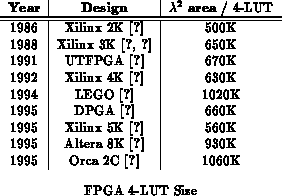
This breakdown, alone, shows us one reason why a full 4-input lookup table is often used as the programmable logic element, rather than a more restricted gate. The area required for the full LUT, including its configuration memory, is less than 10% of the area of the 4-LUT cell, such that there is little advantage to reducing the cell's functional size.
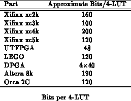
The number of programming bits per 4-LUT for these devices is summarized in
Table . Using a rather large memory cell
(
4.5K
/bit), the memory accounted for 35% of the area
on UTFPGA. With 4-contexts and 600
3T-DRAM memory cells, memory
only occupied 33% of the area on the DPGA. If we assume
1000
static memory cells, for the Xilinx parts, memory accounts for
about 15-30% of that area
(
(32%),
, (15%),
, (32%),
, (21%)).
Making similar assumptions, memory accounts for 21% of an
Altera 8K part (
) and 11%
(
) of an Orca 2C part.
Interconnect and routing occupies the balance of the area
(70-90%).
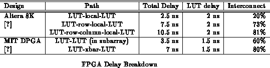
Most vendors lump interconnect timing in with lookup table
evaluation, making it difficult to distinguish the components of delay.
Table summaries interconnect and LUT logic delay
for Altera's 8K series [Alt95] and our own experience with the
DPGA (Chapter
). From here, we see that interconnect typically
accounts for 80% of the path delay.
FPGA networks, which already need to interconnect thousands of independent processing elements, do not, typically, look like conventional multiprocessor networks. In particular, a number of conceptually ``simple'' network structures commonly used as the basis for multiprocessor networks do not scale properly for use in FPGAs. In this section, we review three typical organizations and highlight their shortcomings on the scale required for FPGA networks.
To guarantee arbitrary, full, connectivity among elements, we could build a a full crossbar for the interconnection network. In such a scheme we would not have to worry about whether or not a given network could be mapped onto the programmable interconnect nor would we have to worry about where logic elements were placed. Unfortunately, the cost for this full interconnect is prohibitively high.
For an element array where each element is a
-input function (
e.g.
-LUT), the crossbar would be an
crossbar. Arranged in a roughly square array, each input
and output must travel
distance, before we account for
saturated wire density. Since interconnect delay is proportional to
interconnect distance, this implies the interconnect delay grows at least as
. However, the bisection bandwidth for any full crossbar is
. For sufficiently large
, this bisection bandwidth requires that
the side of an array be
to accommodate the wires across the
bisection. In turn, the
bisection bandwidth dictates an area
. This also dictates input and output wires of length
.
For large crossbars, wire size dominates the areas. These growth rates are
not acceptable even at the level of thousands of LUTs. If we were to build
devices using a single monolithic crossbar for interconnect:
Consider, for the sake of illustration, the size of a crossbar
required to interconnect a 2,500 4-LUT device. We will assume the minimum
wire pitch is 8 and the crossbar is implemented with two layers of
dense metal routed at this minimum wire-pitch. The area of such an array,
as dictated simply by the wiring would be:
Making for an area of
per
4-LUT just to handle the requisite wiring. Conventional FPGAs use a
single SRAM cell to configure each of the crosspoints in the crossbar. If
this were done, the area would be memory bit dominated rather than wire
dominated and take up:
Which results in 10M
per 4-LUT just to hold the configuration
memory. The area per LUT, of course, continues to grow linearly in the
number of LUTs for larger networks.
Multistage interconnection networks ( e.g. butterfly, omega,
CLOS, Benes) can reduce the total number of switches required from to
, but have the same bisection bandwidth problem. Between any two
pair of stages in a butterfly network, the total bisection bandwidth is
, such that the wiring requirements dictate that area grows at
.
At the opposite interconnect extreme, we can use
only local connections within the array between adjacent, or close, array
elements. By limiting all the connections to fixed distances, the link
delay does not grow as the array grows. Further, the bisection bandwidth
in a mesh configuration is and hence, never dominates the
logical array element size. However, communicating a piece of data between
two points in the array requires switching delay proportional to the
distance between the source and the destination. Since switching delay
through programmable interconnect is generally much larger than fanout or
wire propagation delay along a fixed wire, this makes distant communication
slow and expensive. For example, in a topology where direct connections
are only made between an array element and its north, east, south, and west
neighbors (typically called a NEWS network), a
signal must traverse a number of programmable switching elements
proportional to the Manhattan distance between the source and the
destination (
). For the interconnect network topologies
typically encountered in logic circuits, this can make interconnect delay
quite high -- easily dominating the delay through the array element logic.
With this background, we can begin to formulate the design requirements for programmable interconnect:
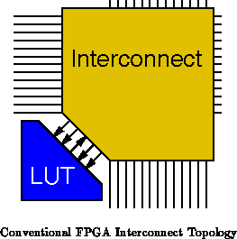
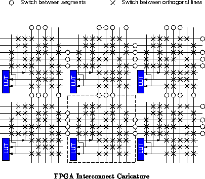
Conventional FPGA interconnect takes a hybrid approach with
a mix of short, neighbor connections and longer connections.
Figure shows a canonical FPGA LUT tile.
Full connectivity is not supported even within the interconnect of a single
tile. Typically, the interconnect block includes:
The University of Toronto has performed a number of empirical interconnect studies aimed at establishing basic FPGA interconnect characteristics, including:
One of the key differences between FPGAs and traditional ``multiprocessor'' networks is that FPGA interconnect paths are locked down serving a single function. The FPGA must be able to simultaneously route all source-sink connections using unique resources to realize the connectivity required by the FPGA. Another key difference is that the interconnection pattern is known a prior to execution, so offline partitioning and placement can be used to exploit locality and thereby reduce the interconnect requirements.
Before we examine how network requirements scale with connectivity
and network size, in this section, we briefly review the number of switches
conventionally employed by networks supporting 100 to 1000 4-LUTs. Brown
and Rose [BFRV92][RB91] suggest each
4-LUT in a moderate sized FPGA with 100's of 4-LUTs will require 200-400
switches. Agarwal and Lewis suggest approximately 100 switches per LUT for
hierarchical FPGAs [AL94] with some reduction in logic
utilization. Conventional, commercial FPGAs do little or no encoding on
their interconnect bit streams -- that is, each interconnect switch is
controlled by a single configuration bit. From the configuration bit
summary in Table , we see that commercial devices also
exhibit on the order of 200 switches per 4-LUT. The fact that conventional
FPGAs can, with difficulty, route most all designs using less than 80-90%
of the device LUTs, suggests that they chose a number of switches
which provides reasonably ``adequate'' interconnect for the current device
sizes -- hundreds to a couple of thousand 4-LUTs.
In Sections
and
, we have empirically
established the size of conventional interconnect. However, as we glimpsed
in Section
, the area which these resources occupy is not
necessarily independent of the number of LUTs interconnected. In this
section we look at how interconnect requirements will grow with the number
of LUTs supported.
The best characterization to date which empirically meters interconnect requirements is Rent's Rule [Vil82][LR71]:
is the number number of interconnection in/out of a region
containing
.
and
are empirical constants. For logic
functions
, typically.
El Gamal used a stochastic model to estimate the interconnection
requirements for channeled gate arrays [Gam81]. He
found that each routing channel requires tracks if the
average wire length,
, grows faster than
.
here is the total number of circuits in the
array, generally arranged in an
array.
Brown used El Gamal's routing model for FPGAs and found good correspondence
between it and FPGA interconnect requirements
[Bro92]. For large numbers of gates
(
) and
, Donath finds that
[Don79]. Together this means
the channel width grows as
. From which we can
derive the interconnect requirements growth:
is often considered a good, conservative, value for
to
handle most interconnect requirements.
For , Donath finds that
grows as
or smaller. For
,
El Gamal's model suggests the the track width grows as
.
In this case, total interconnect requirements grow as
.
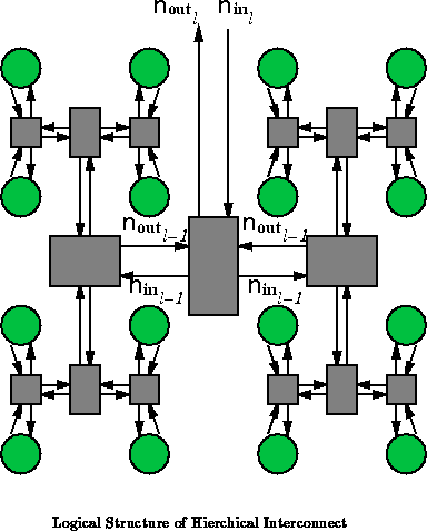
The gates are recursively partitioned into equally sized
sets at each level of the hierarchy. The principal interconnect
occurs at each node of convergence in the hierarchy (See
Figure
). At a level
in the hierarchy, each node
has a fan-in from below of
signals and a fan-in
from above of
. Similarly, it has a fan-out of
toward the leaves and
towards the root. At
each level
, we have
LUTs,
external inputs,
and
external outputs. According to the hierarchical
combining and Rent's Rule growth, we have:
We take , the number of LUT inputs. When
, which will be true for small
, we
take
-- that is, all outputs are passed out of the region
when this Rent bandwidth permits.
Logically, we have distinct output directions from
each node of convergence in the interconnect --
for the
leaves, plus
one for the root. Allowing full connectivity within each tree node, each
of the
leaves picks its
inputs from the
outputs from its siblings and from the
inputs from the parent node. The
outputs of this node
are selected from the
outputs from all
subtrees
converging at this point. Figure
shows this basic
arrangement for
.
First, let us consider how wiring resources grow in this structure.
At each stage of the hierarchy, there are wires coming and leaving each subarray. This makes
the bisection width of
.
For a two-dimensional network layout, this bisection width must cross out
of the subarray through the perimeter. Thus the perimeter of each subarray
is
. The area of the subarrays
will be proportional to the square of its perimeter, making:
The area required for each LUT based on wiring constraints, then, goes as:
Not unsurprisingly, this matches the interconnect growth we derived in
Equation . Of course, if
, wiring is not
the dominant resource constraining LUT area.
may be
for
as far as strict wiring requirements are concerned.
We can also look at the number of switches required if each of the
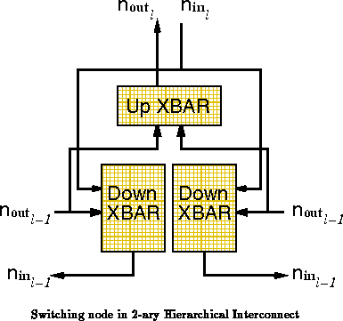
logical switching units is a fully-populated crossbar. At each level, ,
the total number of switches is:
Amortizing across the number of LUTs supported at level , we can count
the number of switches per LUT at each level:
Summing across all levels, we can thus calculate the number of switches per
LUT as a function of the size of the network.
Substituting
for
, and expanding sum:
For , this gives us:
For , each sum term in Equation
goes
to one:
For ,
Putting these cases, together:
Here, we see switching area per LUT grows as , for
, and
for
.
Again, this matches our wiring growth expectations
(Equation
).
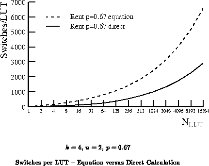
While Equation gives the correct growth
rates it overestimates the required number of switches on two accounts:
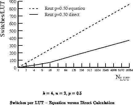
In the previous section, we saw that the amount of interconnect we need to provide depends upon the connectivity of the network. This makes it difficult to design a single network which will efficiently accommodate arbitrary designs. If the design has limited connectivity, but the network provides a large amount of connectivity, the network is over designed relative to the design and provides less functional density than achievable. If the design has considerable connectivity, but the network provides less, the design must be routed sparsely on the interconnect, leaving many of the device LUTs unusable.
Using the switching models derived in the previous section, we can
examine the relative inefficiencies of using a design with Rent exponent
on a network with Rent exponent
. We do this by
looking at the ratio of the area occupied by a design with
LUTs
and on top of a network built using Rent exponent
. If
, then the ratio is simply the ratio of
the area per LUT of a
interconnect of
LUTs to the area
per LUT of a
interconnect of
LUTs. However, if
, we cannot simply map the design netlist on top of the
device LUTs. Here, we have to figure out how much larger the network must
be than the number of LUTs in the design in order to accommodate the highly
connected design. Let us call this scaling factor
. In order for the
network to accommodate the design, it must have enough i/o bandwidth into
each subregion. Starting at the top level in the design, this means:
The only way to accommodate this requirement with a fixed
is to
scale up the network used. Applying Rent's Rule
(Equation
), this means:
Solving this relation for equality:
Note that once we accommodate the top level of the design, all other levels
are also accommodated as well. That is, once we have chosen as above, at
the top level:
Since , at level
, the connectivity required for
the design will shrink faster than the network connectivity, so lower
levels are satisfied by the same scale up factor which satisfies the top
level in the design. The overhead ratio for the
case, then, is the ratio of the size of a
interconnect with
Rent exponent
compared to the size of
an
interconnect with Rent exponent
.
In making this area comparison, we assume that switching area
dominates non-switching area, and we approximate LUT area as proportional to
the number of switches. From Section , we
saw that this is true of conventional devices. In the previous section, we
saw that switching requirements grow at least as fast as wires, and
generally faster than non-switching resources. This suggests that
switching area will continue to dominate non-switching area as device
capacities grow.
If we solve for strictly according to
Equation
, the ratios are continuous and do not take into
account the discretization affects associated with network size and
levels. The continuous approximation gives us a smooth way to compare
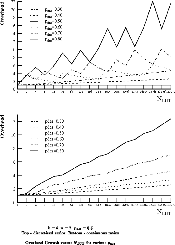
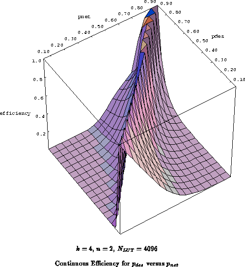
general overhead growth trends. Figure
shows both
the discrete and continuous comparisons for various
implemented on a network with
as a function of
.
Figure
similarly shows the relative overheads for
implementing
designs with
on
designs.
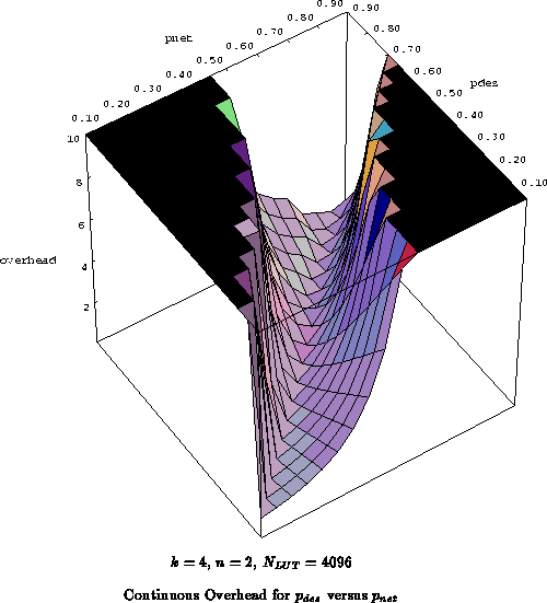
Figure
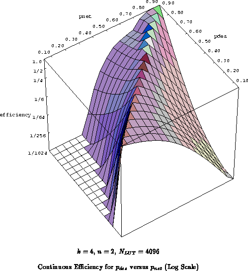
plots the same data as the continuous case from
Figure
on three axes. Figure
plots the
continuous efficiency, the inverse of overhead, and
Figure
plots the continuous efficiency on a
logarithmic scale.
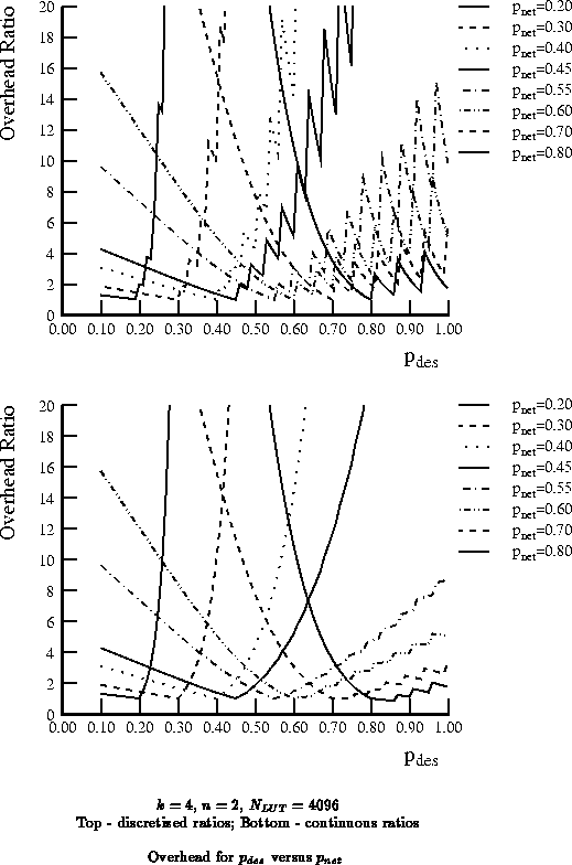
Ideally, we would like to match the programmable network
connectivity to the design connectivity. Unfortunately, we do not
generally get that choice. Figures
through
show us that it is just as inefficient to
provide too much interconnect for a design as it is to provide too little.
This is important to notice, since there is a tendency to demand rich
interconnect that provides high gate utilization across all designs.
However, since the non-interconnect area is trivial compared to network
area in FPGA devices, optimizing for gate utilization is often short
sighted.
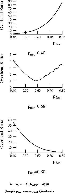
As a final, illustrative example, let us consider the task of
picking the network connectivity, , assuming that we know typical
designs will have a
between 0.4 and 0.8.
Figure
shows the overheads for
values of 0.4,
0.58, and 0.8 as a function of
, respectively. If we further
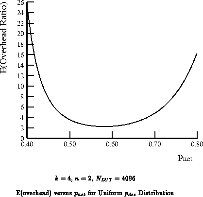
assume that the design Rent exponents are evenly distributed in this range, we
can calculate an expected overhead:
Figure
plots this expected overhead for the identified range.
We see that the expected overhead is quite flat between
=0.5 and
0.6 with an
expected overhead of just over 2
. At the ends of the spectrum, the
expected overhead is 8
worse. Note, in particular, if we
chose to build
in order to guarantee full utilization of
every LUT, we would pay a 16
overhead on average, and a 56
overhead in the worst case. In contrast, choosing
has a
worst-case overhead of 4.2
and an average overhead of 2.2
.
We can also ask how the requirements for interconnect description
will grow. Trivially, we know that it will grow no faster than the number
of switches composing the interconnect. However, it can actually grow much
slower. We start (Section ) by using the
full-connectivity model of the crossbar to establish an upper bound on the
necessary interconnect description length. We then continue
(Section
) using the Rent's rule based hierarchical
interconnect, as in previous sections, to derive a tighter
approximation. By either metric, we see that the instruction sizes for
conventional FPGAs are significantly larger than necessary. This
observation suggests that context memory area and reload instruction
bandwidth can be significantly reduced by judicious coding
(Section
).
Assuming that the network may be arbitrarily connected, we can count the number of possible interconnection patterns to get an upper bound on the number of interconnection bits which can be usefully employed describing the input to each LUT. We start by assuming we have a device composed of:
Since a LUT has inputs, the total number of interconnect bits needed is
simply:
e.g. A 1000 4-LUT device with 200 inputs would require only 41 bits (44 if we encode each input separately) to specify each LUT's interconnect. A 9000 4-LUT device with 600 inputs requires only 53 bits (56 for separate input encodings).
If our functional elements are truly 4-LUTs, then this upper bound
can be tightend by noticing that we gain no additional functionality by
being able to route a particular source into the LUT multiple times and the
assignment of the sources to LUT inputs is inconsequential. With this
observation, we really only need to choose items from
when specifying the LUT interconnect. This gives:
e.g. our 1000 4-LUT device with 200 inputs requires only 37 bits and our 9000 4-LUT device with 600 inputs requires only 49 bits. Here we save an additional 4 bits per 4-LUT. Asymptotically:
So, we expect that exploiting the equivalence of the inputs on a
-LUT to save us
bits from the number of bits required for
full interconnect. For
, this amounts to a savings of 4-5 bits per
LUT.
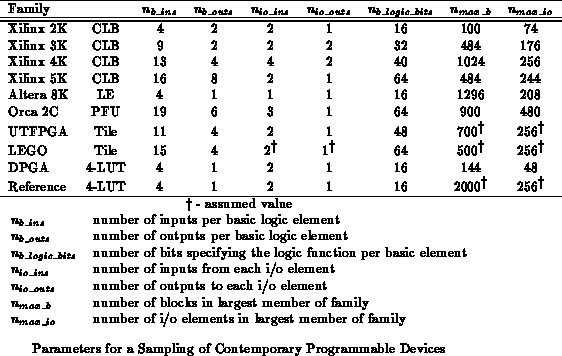
Commercial devices are not purely composed up of LUTs, but we can
draw a box around their basic programming elements and use the above
counting arguments to get a loose upper bound on the number of interconnect
programming bits they could require. Table shows
parameters for each of several commercial device families along with a
pedagogical reference. Using the parameters given in
Table
, we can use the full connectivity assumption to
compute an upper bound on the network description length:
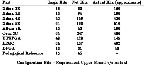
Table calculates
for each
of the device families from Table
and contrasts these
numbers with the number of actual device bits per basic element.
The comparison is necessarily crude since vendors do not provide detailed
information on their configuration streams. However, we expect the
unaccounted control bits in Table
to not be more than
10% of the total bits per block.
With this expectation, we see that the commercial devices exhibit a factor
of two to three more interconnect configuration bits than would be required
to provide full, placement-independent, interconnect of the logic blocks.
The upper bound derived in the previous section assumed full
connectivity of the network. However, the network is generally much more
restricted. The restrictions imply a smaller class of realizable
connection patterns and fewer requisite interconnect bits. In this section
we return to our pedagogical, hierarchical interconnect from
Section . For small Rent exponents,
, we can derive
tighter bounds.
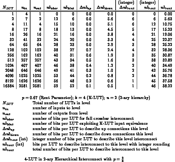
Reconsidering, the hierarchical interconnect structure from
Figures and
, we can calculate the
number of bits required per level of the hierarchy.
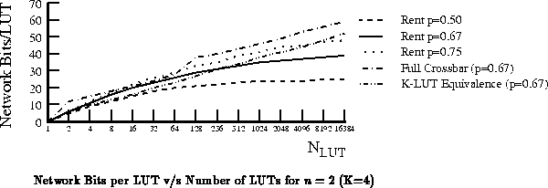
Table summarizes these values by level for
, along with the number of bits according to the earlier
crossbar and K-LUT equivalence calculations. This scheme also gives only
an upper bound since the individual treatment of the permutations within
each level counts more distinct combinations than actually exist. For
moderate values of
, though, this will give a tighter bound than the
crossbar bound derived in the previous section.
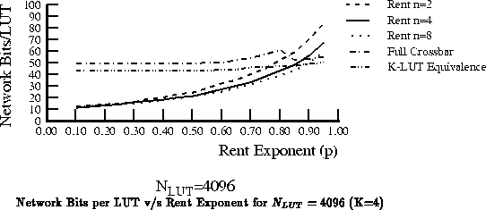
The number of bits required will vary with the Rent exponent .
Figure
shows this variation. It also shows the
relationship among choices of the arity of the hierarchy,
, and the
crossbar and K-LUT equivalence bounds. Figure
shows
the growth rate versus the number of LUTs for several Rent exponents and
the two crossbar bounds.
Note that Donath performs a similar calculation in
[Don74]. He uses a more restrictive interconnect model.
Using 2- to 3-input, single-function gates, he calculates 7-10 bits of
memory per to 0.8. In Donath's model, the required description
bits does not grow with network size.
Resources for instruction storage and distribution, as the next
Chapter (Chapter ) will address, can take up significant
area and play a big role in the characteristics of an architecture.
Notably, the size of the instruction determines the size of the instruction
store on and off chip and the bandwidth required to load new instructions.
The bounds we derived in the previous sections show that the
instruction sizes in traditional FPGAs are higher than necessary, at least
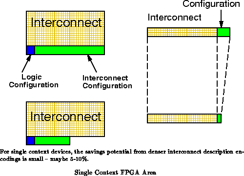
by a factor of 2-4. For single context devices as we have seen,
instruction memory makes up only a small fraction of the area on a
conventional FPGA. For this reason, these bloated instructions do not
adversely affect FPGA cell area (See Figure
). In fact,
in wire limited regimes, they may help by localizing instruction bits to
the values they control.
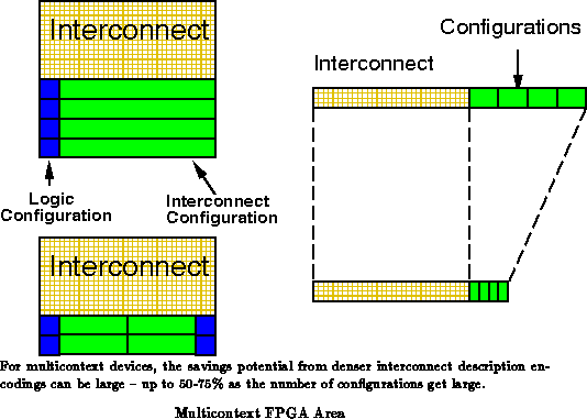
The most significant impact is on reconfiguration time. Smaller instructions mean we can reload instructions in less time, given the same bandwidth for instruction reload. Alternately, it means that correspondingly less resources can be dedicated to instruction distribution in order to achieve the same instruction reload time as the larger instructions.
As we begin to make heavy use of the reconfigurable aspects of programmable devices, device reconfiguration time becomes an important factor determining the performance provided by the part. In these rapid reuse scenarios, instruction size can play a significant role in determining device area and performance.
From the previous sections, we have seen that interconnect requirements grow faster than interconnect description requirements. Specifically:
This is one reason that single context devices can afford to use sparse interconnect encodings. Since the wires and switches are the dominant and limiting resource, additional configuration bits are not costly. In the wire limited case, we may have free area under long routing channels for memory cells. In fact, dense encoding of the configuration space has the negative effect that control signals must be routed from the configuration memory cells to the switching points. The closer we try to squeeze the bit stream encoding to its minimum, the less locality we have available between configuration bits and controlled switches. These control lines compete with network wiring, exacerbating the routing problems on a wire dominated layout.
So far, we have looked entirely at single-bit level granularity networks and designs. In this section, we look at how the multi-bit designs and networks effect the relations we have already developed.
In general, we will assume a -bit datapath with
total
bit processing elements. Groups of
bit processing elements will act
as a single compute node. We thus have
such compute nodes.
We look at the wiring requirements, as we did before, by looking
at the bisection bandwidth implied by the network. Assuming Rent's rule
based hierarchical interconnect, at the top level we have
i/o busses of width
. This makes for a total bisection bandwidth:
This makes the wire dictated area growth go as:
Per LUT this makes:
Notice that this is actually larger than the interconnect wiring area
required for single-bit interconnects (Equation ).
This result makes the assumption that the bits composing a node
are tightly interconnected or otherwise coupled such that the minimum
bisection occurs between tree levels as before. If the
bits in a node
were not interconnected in any way, the network could be decomposed into
single bit networks. In such a case, the size would simply be
times the size of an
single bit network, making:
Equation implies the area
is actually smaller than the single bit network for
.
In practice the earlier result (Equation
) is most
realistic.
One issue this raises is that a -bit design with Rent exponent
implemented on top of a single bit network will require more
interconnect per level than a single bit design with Rent exponent
.
Using the same technique as in Section
, we can solve
for the required scale up factor:
Switching requirements, in contrast, diminish with increasing
since less flexibility is required of the network with a given number of bit
processing elements. We can derive the switching requirements by
substituting
in for
in
Equation
then multiplying by the datapath width:
For large , wiring requirements will asymptotically dominate
switching requirements in a bussed interconnect scheme.
This section focussed on interconnect. We established via an
empirical review that interconnect makes up the dominant area and delay in
conventional FPGAs. We then went on to look at network design issues. We
established basic relations governing the interconnect requirements in
terms of network size and wiring complexity. In the processes we showed
that it is not always best to build the network with sufficient interconnect to
accommodate the most heavily interconnected designs at full gate utilization;
rather, since interconnect is the dominant area contributor, more efficient
area utilization can be achieved with networks with lower interconnect
complexity. We also looked at interconnect description requirements,
noting that interconnect descriptions grow more slowly than wire and
switching requirements. Here, we pointed out that conventional devices use
sparse interconnect description encodings, using, at least a factor of
2-4 more configuration bits than necessary; this observation
suggests that we have an opportunity to reduce the area required to hold
descriptions in multicontext devices and the bandwidth required for
configuration reload in single or multicontext devices. Finally, we looked
at how the interconnect size relationships change with wider word
operations and saw that greater word widths increase wiring requirements
while decreasing switching requirements.