Previous: Dynamically Programmable Gate Arrays with Input Registers Up: New Architectures Next: MATRIX
We established in Chapter that active
interconnect area consumed most of the space on traditional, single-context
FPGAs. In Chapter
, we saw that adding small, local, context
memories allowed us to reuse active area and achieve smaller task
implementations. Even in these multicontext devices, we saw that
interconnect consumed most of the area
(Section
). In Chapter
, we added
architectural registers for retiming and saw more clearly the way in which
multiple context evaluation saves area primarily by reducing the need for
active interconnect. In this chapter, we describe the Time-Switched Field
Programmable Gate Array (TSFPGA), a multicontext device designed explicitly
around the idea of time-switching the internal interconnect in order to
implement more effective connectivity with less physical interconnect.
One issue which we have not addressed in the previous sections is the complexity of physical mapping and, consequently, the time it takes to perform said mapping. Because of the computational complexity, physical mapping time can often be the primary performance bottleneck in the edit-compile-debug cycle. It can also be the primary obstacle to achieving acceptable mapping time for large arrays and multi-chip systems.
In particular, when the physical routing network provides limited interconnectivity between LUTs, it is necessary to carefully map logical LUTs to physical LUTs in accordance with both netlist connectivity and interconnect connectivity. The number of ways we can map a set of logical LUTs to a set of physical LUTs is exponential in the the number of mapped LUTs, making the search for an acceptable mapping which simultaneously satisfies the netlist connectivity constraints and the limited physical interconnect constrains -- i.e. physical place and route -- computationally difficult. Finding an optimal mapping is generally an NP-complete problem. Consequently, in traditional FPGAs, this mapping time can be quite large. It often take hours to place and route designs with a couple of thousand LUTs. The computational complexity arises from two features of the mapping problem:
This chapter details a complete TSFPGA design including:
As noted in Section , if all retiming can be
done in input registers, only a single wire is strictly needed to
successfully route the task. The simple input register model used for the
previous chapter had limited temporal range and hence did not quite provide
this generality. In this section, we introduce an alternative input
strategy which extends the temporal range on the inputs without the linear
increase in input retiming size which we saw with the shift-register based
input microarchitecture in the previous chapter.
The trick we employ here is to have each logical input load its value from the active interconnect at just the right time. As we have seen, multicontext evaluation typically involves execution of a series of microcycles. A subset of the task is evaluated on each microcycle, and only that subset requires active resources in each microcycle. We call each microcycle a timestep and, conceptually at least, number them from zero up to the total number of microcycles required to complete the task. If we broadcast the current timestep, each input can simply load its value when its programmed load time matches the current timestep.
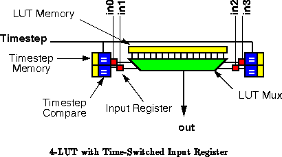
Figure shows a 4-LUT with this input arrangement
which we will call the Time-Switched Input Register. Each LUT input
can load any value which appears on its input line in any of the last
cycles. The timestep value is
bits
wide, as is the comparator. With this scheme, if the entire computation
completes in
timesteps, all retiming is accomplished by simply loading
the LUT inputs at the appropriate time -- i.e. loading each input
just when its source value has been produced and spatially routed to the
destination input. Since the hardware resources required for this scheme
are only logarithmic in the total number of timesteps, it may be reasonable
to make
large enough to support most all desirable computations.
With this input structure, logical LUT evaluation time is now
decoupled from input arrival time. This decoupling was not true in FPGAs,
DPGAs, or even iDPGAs. With FPGAs, the LUT is evaluated only while the
inputs are held stable. With DPGAs, the LUT is evaluated only on the
microcycle when the inputs are delivered. With the iDPGA, the LUT must be
evaluated on the correct cycle relative to the arrival of the input, and
the range of feasible cycles was limited by . Further, with the
time-switched input register, the inputs are stored, allowing the LUT
result to be produced on any microcycle, or microcycles, following the
arrival of the final input. In the extreme case of a single wire for
interconnect, each LUT output would be produced and routed on a separate
microcycle. Strictly speaking, of course, with a single wire there need be
only one physical LUT, as well.
This decoupling of the input arrival time and LUT evaluation time
allows us to remove the simultaneous constraints which, when coupled with
limited interconnectivity, made traditional programmable gate array mapping
difficult. We are left with a single constraint: schedule the entire task
within timesteps.
Conceptually, let us consider array interconnect as composed of a
series of fully interconnected subarrays. That is, we arrange groups of
LUTs in subarrays, as in the DPGA prototype (See
Section ). Within a subarray, LUTs are fully
interconnected with a monolithic crossbar. Also feeding into and out of
this subarray crossbar are connections to the other subarrays.
The subarray contains a number of LUTs, , where we
consider
as typical. Connecting into the subarray are
inputs from outside. Similarly,
connect out.
, and
are typically governed by Rent's Rule. With
,
, and
, we might expect
, and consider
typical and convenient.
Together, this suggests a crossbar, which is
for the typical values listed above. This amounts to 640
switches per 4-LUT, which is about 2-3
the values used in
conventional FPGA architectures as we reviewed in
Section
. Conventional
architectures, effectively, only populate 30-50% of the switches in such a
block relying on placement freedom to make up for the missing switches. It
is, of course, the complexity of the placement problem in light of this
depopulation which is largely responsible for the difficulty of place and
route on conventional architectures.
We also need to interconnect these subarrays. For small arrays it
may be possible to simple interwire the connections between subarrays
without substantial, additional switching. This is likely the case for the
100-1000 LUT cases reviewed in
Section . For larger arrays, more,
inter-array switching will be required to provide reasonable connectivity.
As we derived in Section
, the interconnect requirements will
grow with the array size.
With switched interconnect, we can realize a given level of connectivity without placing all of the physical switches that such connectivity implies. Rather, with the ability to reuse the switches, we effect the complete connectivity over a series of microcycles.
We can view this reuse as a folding of the interconnect in time.
For instance, we could map pairs of LUTs together such that they share input
sets. This, coupled with cutting the number of array outputs
() in half, will cut the number of crossbar outputs in half
and hence halve the subarray crossbar size. For full connectivity, it may
now takes us two microcycles to route the connections, delivering the inputs
to half the LUTs and half the array outputs in each cycle. In this
particular case we have performed output folding by sharing crossbar
outputs (See Figure
). Notice that the time-switched input
register allows us to get away with this
folding by latching and holding values on the correct microcycle. The
input register also allows the non-local subarray outputs to be transmitted
over two cycles. In the most trivial case, the array outputs will be
connected directly to array inputs in some other array and, through the
destination array's crossbar, they will, in turn be connected to LUT inputs
where they can be latched on the appropriate microcycle as they arrive.
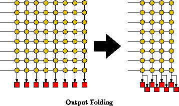
There is one additional feature worth noting about output folding. When two or more folded LUTs share input values all the LUTs can load the input when it arrives. For heavily output folded scenarios, these shared inputs can be exploited by appropriate grouping to allow the task to be routed in less microcycles than the total network sharing.
We can also perform input folding. With input
folding, we pair LUTs so that they share a single LUT output. Here
we cut the number of array inputs () in half, as well. The
array crossbar now requires only half as many inputs as before and is,
consequently, also half as large in this case. Again, the latched inputs
allow us to load each LUT input value only on the microcycle on which the
associated value is actually being routed through the crossbar. For input
folding, we must add an effective pre-crossbar multiplexor so that we can
select among the sources which share a single crossbar input (See
Figure
).
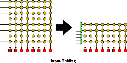
It is also possible to fold together distinct functions. For example, we could perform an input fold such that the 64 LUT outputs each shared a connection into the crossbar with the 64 array inputs. Alternately, we could perform an output fold such that LUT inputs shared their connections with array outputs.
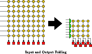
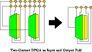
Finally, note that we can perform input folding and output folding
simultaneously (See Figure ). We can think of the DPGAs
introduced in Chapter
as folded interconnect where we folded
both the network input and output
times. Each DPGA array element (See
Figure
) shared
logical LUT inputs on one set of physical
LUT inputs and shared
logical LUT outputs on a single LUT output.
Figure
shows how a two context DPGA results from a
single input and output fold. In the DPGA, we had only
routing
contexts for this
total folding. To get away with this factor of
reduction in interconnect description, we had to restrict routing to
temporally adjacent contexts. As we saw, in Chapter
this
sometimes meant we had to allocate LUTs for through routing when
connections were needed between contexts.
Routing on these folded networks naturally proceeds in both space and time. This gives the networks the familiar time-space-time routing characteristics pioneered in telephone switching systems.
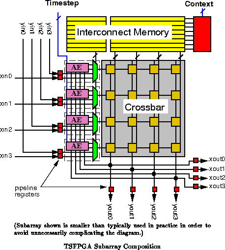
In this section, we detail a complete TSFPGA architecture. The
basic TSFPGA building block is the subarray tile (See
Figure ) which contains a collection of LUTs and a central
switching crossbar. LUTs share output connections to the crossbar and
input connections from the crossbar in the folded manner described in the
previous section. Communication within the subarray can occur in one
TSFPGA clock cycle. Non-local input and output lines to other subarrays
also share crossbar I/O's to route signals anywhere in the device. Routes
over long wires are pipelined to maintain a high basic clock rate.
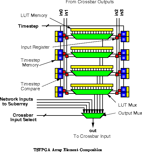
The LUT input values are stored in time-switched input registers. The inputs to the array element are run to all LUT input registers. When the current timestep matches the programmed load time, the input register is enabled to load the value on the array-element input. When multiple LUTs in an array element take the same signal as input, they may be loaded simultaneously.
Unlike the DPGA architectures detailed in Chapters
and
, the LUT multiplexor is replicated for each logical LUT.
As we saw in Section
, the LUT mux is only a tiny
portion of the area in an array. Replicating it along with context memory
avoids the need for final LUT input multiplexors which would otherwise be
in the critical path. When considering both the additional input
multiplexors and the requirements for selecting among the LUT programming
memory, the benefit of resource sharing at this level have been minimal in
most of the implementations we have examined.
The primary switching element is the subarray crossbar. As shown in
Figures and
, each crossbar input is
selected from a collection of subarray network inputs and subarray LUT
outputs via by a pre-crossbar multiplexor. Subarray inputs are registered
prior to the pre-crossbar multiplexor and outputs are registered
immediately after the crossbar, either on the LUT inputs or before
traversing network wires. This pipelining makes the LUT evaluations and
crossbar traversal a single pipeline stage. Each registered, crossbar
output is routed in several directions to provide connections to other
subarrays or chip I/O.
Inter-subarray wire traversals are isolated into a separate
pipeline stage between crossbars. As we saw both in
Section and the DPGA
prototype implementation (Section
), wire and
switch traversals are responsible for most of the delay in programmable
gate arrays. By pipelining routes at the subarray level, we can achieve a
smaller microcycle time and effectively extract higher capacity from our
interconnect.
Notice that the network in TSFPGA is folded such that the single subarray crossbar performs all major switching roles:
Communication within the subarray is simple and takes one clock cycle per LUT evaluation and interconnect. Once a LUT has all of its inputs loaded, the LUT output can be selected as an input to the crossbar, and the LUT's consumers within the subarray may be selected as crossbar outputs. At the end of the cycle, the LUT's value is loaded into the consumers' input registers, making the value available for use on the next cycle.
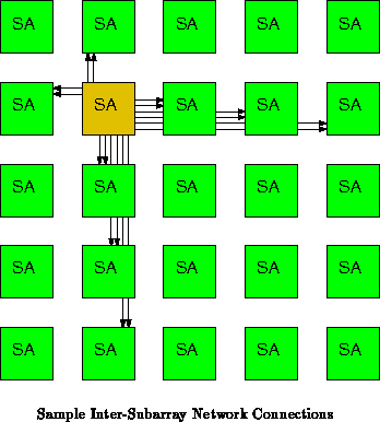
Figure shows the way a subarray may be connected to other
subarrays on a component. A number of subarray outputs are run to each
subarray in the same row and column. For large designs, hierarchical
connections may be used to keep the bandwidth between subarrays reasonable
for while maintaining a limited crossbar size and allowing distant
connections. The hierarchical connections can give the logical effect of a
three or four dimensional network.
Routing data within the same row or column involves:
Two ``instruction'' values are used to control the operation of each
subarray on a per clock cycle basis, timestep and routing
context (shown in Figure ). The routing context serves as
an instruction pointer into the subarray's routing memory. It selects the
configuration of the crossbar and pre-crossbar multiplexors on each cycle.
timestep denotes time events and indicates when values should be
loaded from shared lines.
These two values are distinct in order to allow designs which take more microcycles to complete than they actually require contexts. The evaluation of a function will take a certain number of TSFPGA clock cycles. This time is dictated by the routed delay. For designs with large serial paths, long critical paths, or poor locality of communications, the routed delay may be large without consuming all the routing resources. For this reason, it is worthwhile to segregate the notion of timestep from the notion of routing contexts. Each routing interconnect pattern, or context, may be invoked multiple times at different timesteps during an evaluation. This allows us to have a small number of routing contexts even when the design topology necessitates a large number of timesteps.
As a trivial example, consider the case of an unfolded subarray. With full subarray interconnect there may be enough physical interconnect in a single context to actually route the complete design. However, since the design has a critical path composed of multiple LUT delays, it will take multiple microcycles to evaluate. In this case, it is not necessary to allocate separate routing contexts for each timestep as long as we segregate these two specifications into separate entities.
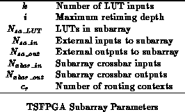
The subarray composition effectively determines the makeup of a
TSFPGA component. Table summarizes the base parameters
characterizing a TSFPGA subarray implementation. From these, we can
calculate resource size and sharing:
Assuming we need to route through one intermediate subarray, on
average, the number of routing contexts, , needed for full connectivity
is:
That is, we need one context to drive each crossbar source for each
crossbar sink. When we have the same number of contexts as we have total
network sharing, we can guarantee to route anything.
Relation assumes that
and
are chosen reasonably large to support traffic to, from, and through the
array. If not, the sharing of inter-subarray network lines will dominate
strict crossbar sharing, and should be used instead.
In practice, we can generally get away with less contexts than
implied by Relation by selectively routing outputs and
inputs as needed. When LUT inputs sharing a crossbar output also share
input values or when the mapped design requires limited connectivity, less
switching is needed, and the routing tasks can be completed with fewer
contexts. The freedom to specify which output drives each crossbar input
on a given cycle, as provided by the TSFPGA subarray, is not strictly
necessary. We could have a running counter which enables each source in
turn. However, with a fixed counter it would always take
cycles to pull out any particular source, despite the
fact that only a few are typically needed at any time. The effect is
particularly acute when we think about levelized evaluation where we may be
able to simultaneously route all the LUTs whose results are currently ready
and needed in a single cycle. For this reason, TSFPGA provides independent
control over the pre-crossbar input mux.
In total, the number of routing bits per LUT, then, is:
Additionally, each LUT has its own programmable function and matching inputs:
The time-switched input register is the most novel building block in the TSFPGA design. A prototype layout by Derrick Chen was:
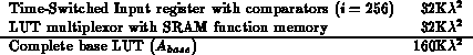
Note that contains the LUT multiplexor, LUT function memory,
all
input registers, their associated comparators, and the comparator
programming.
The amortized area per LUT then is:
Using the subarray as a reference,
a version with no folding has,
,
, making
, which is about
2-3
the size of typical 4-LUTs. But, as we noted above, unfolded,
we have 2-3
as many switches as a conventional FPGA implementation.
Also, unfolded, the expensive, matching input register is not needed.
If we fold the input and output each once, ,
, the number of switches drops to
.
With four routing contexts (
), routing bits rise to
. The total area is
, which is comparable in size with modern FPGA
implementations, while providing 2-3
the total connectivity.
At this size, each TSFPGA 4-LUT is effectively larger than the
logical 4-LUT area in the iDPGAs of the previous chapter. The added
complexity and range () of the time-switched input registers is
largely responsible for the greater size. The time-switched input register
features, in turn, are what allow us map designs without satisfying a
large number of simultaneously constraints.
Within the subarray, the critical path for the operating cycle of this design point contains:
Traditional logic and state-element netlists can be mapped to TSFPGA for levelized logic evaluation similar to the DPGA mapping in the previous two chapters. Using this model, only the final place-and-route operation must be specialized to handle TSFPGA's time-switched operation. Of course, front-end netlist mapping which takes the TSFPGA architecture into account may be able to better exploit the architecture, producing higher performance designs.
tspr, our first-pass place-and-route tool for TSFPGA, performs placement by min-cut partitioning and routing by a greedy, list-scheduling heuristic. Both techniques are employed for their simplicity and mapping-time efficiency rather than their quality or optimality. The availability of adequate switching resource, expandable by allocating more configuration contexts, allows us to obtain reasonable performance with these simple mapping heuristics. For the most part, the penalty for poor quality placement and routing in TSFPGA is a slower design, not an unroutable design.
The topology of the circuit will determine the critical path length, or the number of logical LUT delays between the inputs and outputs of the circuit. This critical path length is one lower bound on the number of timesteps required to evaluate a circuit. However, once placed onto subarrays, there is another, potentially longer, bound, the distance delay through the network. The distance delay is the length of the longest path through the circuit including the cycles required for inter-subarray routing. If all the LUTs directly along every critical path can be mapped to a single subarray, it is possible that the distance delay is equal to the critical path length. However, in general, the placed critical path crosses subarrays resulting in a longer distance delay. The quality of the distance delay is determined entirely during the placement phase.
The actual routed delay is generally larger than the distance delay because of contention. That is, if the architecture does not provide enough physical resources to route all the connections in the placed critical path simultaneously, or the if the greedy routing algorithms allocates those resources suboptimally, signals may take additional microcycles to actually be routed.
For the fastest mapping times, no sophisticated placement is done. Circuit netlists are packed directly into subarrays as they are parsed from the netlists. Such oblivious placement may create unnecessarily long paths by separating logically adjacent LUTs and may create unnecessary congestion by not grouping tightly connected subgraphs. However, with enough routing contexts the TSFPGA architecture allows us to succeed at routing with such poor placement.
Routing is directed by the circuit netlist topology using a greedy, list-scheduling heuristic. At the start, a ready list is initialized with all inputs and flip-flop outputs. Routing proceeds by picking the output in the ready list which is farthest from the end set of primary outputs and flip-flop inputs. Routing a signal implies reserving switch capacity in each context and timestep involved in the route. If a route cannot be made starting at the current evaluation time, the starting timestep for the route is incremented and the route search is repeated. Currently, only minimum distance routes are considered. Assuming adequate context memory, every route will eventual succeed. Once a route succeeds, any LUT outputs which are then ready for routing are added to the ready list. In this manner, the routing algorithm works through the design netlist from inputs to outputs, placing and routing each LUT as it is encountered.
The total number of contexts is dictated by the amount of contention for shared resources. Since some timesteps may route only a few connections, a routing context may be used at multiple timesteps. In the simplest case, switches in a routing context not used during one timestep may be allocated and used during another. In more complicated cases, a switch allocated in one context can be reused with the same setting in another routing context. This is particularly useful for the inter-subarray routing of patterns, but may be computationally difficult to exploit.
Our experimental mapping software can share contexts among routing
timesteps by modulo context assignment. That is context is used to route on timestep
. As we will see in
the next section, this generally allows us to reduce the number of required
contexts. Further context reduction is possible when we are willing to
increase the number of timesteps required for evaluation. More
sophisticated sharing schemes are likely to be capable of producing better
results.
In this section we show the results of mapping the same MCNC benchmark circuit suite used for the DPGA in the previous two chapters to TSFPGA. These benchmarks are mapped viewing TSFPGA simply as an FPGA with time-switched interconnect, ignoring the way one might tailor tasks to take full advantage of the architecture.
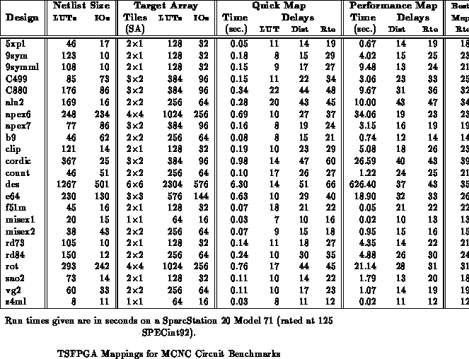
Table shows the results of mapping the benchmark
circuits to TSFPGA. The same area mapped circuits from sis and
Chortle used in Sections
and
were used for this mapping. Each design was
mapped to the smallest rectangular collection of subarray tiles which
supported both the design's I/O and LUT requirements. Quick mapping does
oblivious placement while the performance mapping takes time to do
partitioning. Both the quick and performance map use the same, greedy
routing algorithm. As noted in Section
, fairly simple
placement and routing techniques are employed, so higher quality routing
results are likely with more sophisticated algorithms. Quick mapping can
route designs in the order of seconds, while performance mapping runs in
minutes. The experimental mapping software implementation has not been
optimized for performance, so the times shown here are, at best, a loose
upper bound on the potential mapping time. The ``Best map'' results in
Table
summarize the best results seen over several runs of
the ``performance'' map.
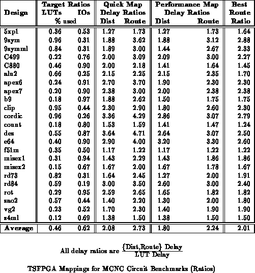
Table shows usage and time ratios derived
from Table
. All of the mapped delay ratios are normalized
to the number of LUT delays in the critical path. We see that the quick mapped
delays are almost 3
the critical path LUT delay, while the
performance mapped delays are closer to 2
. As we noted in
Section
, the basic microcycle on TSFPGA is half that on
the DPGA, suggesting that the performance mapped designs achieve roughly
the same average latency as full, levelized evaluation on the DPGA.
We can see from the distance delay averages that placement dictated delay
is responsible for a larger percentage of the difference between critical
path delay and routed delay. However, since the routed delay is larger
than the distance delay, network resource contention and suboptimal routing
are partially responsible for the overall routed delay time.
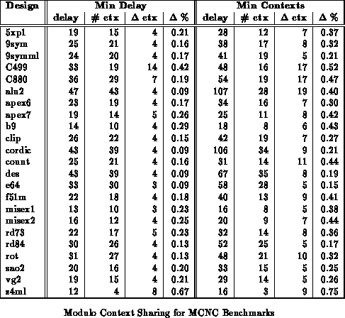
As noted in Section we can use modulo context
assignment to pack designs into fewer routing contexts at the cost of
potentially increasing the delay. Table
shows the
number of contexts into which each of the designs in Table
can be packed both with and without expanding their delay.
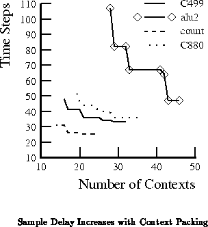
Figure
shows how routed delay of several benchmarks
increases as the designs are packed into fewer routing contexts.
Dharma [BCK93] time-switched two monolithic crossbars.
It made the same basic reduction as the DPGA -- that is, rather than having
to simultaneously route all connections in the task, one only needed to
route all connections on a single logical evaluation level. To make
mapping fast, Dharma used a single monolithic crossbar. For arrays of
decent size, the full crossbar connecting all LUTs at a single level can
still be prohibitively large. Further, Dharma had a rigid assignment of
LUT evaluation and hence routing resources to levels. As we see in TSFPGA,
it is not always worth dedicating all of one's routing resources, an entire
routing context, to a single evaluation timestep. Dharma deals with
retiming using a separate flow-through crossbar. While the flow through
retiming buffers are cheaper than full LUTs, they still consume active
routing area which is expensive. As noted in Chapter , it is
more area efficient to perform retiming, or temporal transport, in
registers than to consume active interconnect.
VEGA [JL95], noted in Sections
and
, uses a 1024 deep context memory, essentially
eliminating the spatial switching network, and uses a register file to
retime intermediate data. The VEGA architecture allows similar
partitioning and greedy routing heuristics to be used for mapping.
However, the heavy multicontexting and trivial network in VEGA means that
it achieves its simplified mapping only at the cost of a 1024
reduction in active peak capacity and 100
penalty in typical
throughput and latency over traditional FPGA architectures.
PLASMA [ACC +96] was built for fast mapping of logic in
reconfigurable computing tasks. It uses a hierarchical series of heavily
populated crossbars for routing on chip. The existence of rich,
hierarchical routing makes simple partitioning adequate to satisfy
interconnect constraints. The heavily populated crossbars make the routing
task simple. The basic logic primitive in PLASMA is the PALE, which is
roughly a 2-output 6-LUT. The PLASMA IC packs 256 PALEs into
16.2mm16.2mm in a 0.8
CMOS process, or roughly 1.6G
.
This comes to 6.4M
per PALE. If we generously assume each PALE
is equivalent to 8 4-LUTs, the area per 4-LUT is 800K
, which is
commensurate with conventional FPGA implementations, or about 2-2.5
the size for the TSFPGA design point described above. In practice, the
TSFPGA LUT density will be even greater since it is not always the case
that 8 4-LUTs can be packed into each PALE. PLASMA's size is a direct
result of the fact that it builds all of its rich interconnect as active
switches and wires. Routing is not pipelined on PLASMA, and critical paths
often cross chip boundaries. As a result, typical PLASMA designs run with
high latency and a moderately slow system clock rate (1-2 MHz). This
suggests a time-switched device with a smaller amount of physical
interconnect, such as TSFPGA, could provide the same level of mapping speed
and mapped performance in substantially less area.
Virtual Wires [BTA93] employs time-multiplexing to extract higher capacity out of the I/O and inter-chip network connections only. Virtual Wires folds the FPGA and switching resources together, using FPGAs for inter-FPGA switching as well as logic. Since Virtual Wires is primarily a technique used on top of conventional FPGAs, it does accelerate the task of routing each individual FPGA or provide any greater use of on-chip active switching area.
Li and Cheng's Dynamic FPID [LC95] is a time-switched Field-Programmable Interconnect Device (FPID) for use in partial-crossbar interconnection of FPGAs. Similarly, they increase switching capacity, and hence routability and switch density, by dynamically switching a dedicated FPID.
UCSB researchers [cLCWMS96] consider adding a second routing context to a conventional FPGA routing architecture. Using a similar circuit benchmark suite, they find that the second context reduces wire and switching requirements by 30%. Since they otherwise use a conventional FPGA architecture, there is no reduction in mapping complexity for their architecture.
We have developed a new, programmable gate-array architecture model based around time-switching a modest amount of physical interconnect. The model defines a family of arrays with varying amounts of active interconnect. The key, enabling feature in TSFPGA is an input register which performs a wide range of signal retiming, freeing the active interconnect from performing data retiming or conveying data at rigidly defined times. Coupling the flexible retiming with reusable interconnect, we remove most of the constraints which make the place and route task difficult on conventional FPGA architectures. Consequently, even large designs can be mapped onto a TSFPGA array in seconds. More sophisticated mapping can be used, at the cost of longer mapping times, to achieve the lowest delay and best resource utilization. We demonstrated the viability of this fast mapping scheme by developing experimental mapping software for one design point and mapping traditional benchmark circuits onto these arrays. At the heavily time-switched design point which we explored in detail, the basic LUT size is half that of a conventional FPGA LUT while mapped design latency is comparable to the latency on fully levelized DPGAs.
At this point, we have left a number of interesting issues associated with TSFPGA unanswered.