
Transit Note #118
Notes on Coupling Processors with Reconfigurable Logic
Andre DeHon
Original Issue: March, 1995
Last Updated: Sat Apr 8 20:35:54 EDT 1995

Introduction
This is an informal note which discusses several options for
incorporating reconfigurable logic into a microprocessor design. The goal
of this note is to catalog and discuss the options. See (tn100)
for a more motivational introduction to coupling reconfigurable arrays with
microprocessors.
The note start by looking at several general classes of
reconfiguration which might be worthwhile to support.
Section  examines reconfigurable i/o, Section
looks at reconfigurable or programmable functional units,
Section described reconfigurable control logic,
Section explores reconfigurable instruction decoding,
and Section looks at scenarios where the processor's basic
behavior is reconfigurable. Section touches on
reconfigurable logic technologies. Section looks at
interface issues associated with reconfiguring the logic.
examines reconfigurable i/o, Section
looks at reconfigurable or programmable functional units,
Section described reconfigurable control logic,
Section explores reconfigurable instruction decoding,
and Section looks at scenarios where the processor's basic
behavior is reconfigurable. Section touches on
reconfigurable logic technologies. Section looks at
interface issues associated with reconfiguring the logic.
Flexible I/O

A large class of interesting applications arise if we insert the
flexible logic into the processor's on/off chip datapath. In the extreme,
the flexible logic could completely replace the off-chip i/o circuitry.
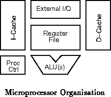
Figure shows the basic organization of a vanilla
microprocessor. The variants described in this section provide
various flexible logic alternatives for the external I/O interface.
Architectural Options
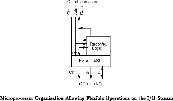
Figure shows a scenario where the flexible logic can
interpose itself in the i/o operation. Arranged appropriately, the
latency impact on i/o operations which do not make use of the
reconfigurable logic can be minimal
-- just an extra multiplexor delay in each path. When the reconfigurable
array processes data on its way on or off chip, the reconfigurable
processing can be pipelined with processor and i/o operations. The
reconfigurable operations will increase the off chip latency, but not
diminish bandwidth. Of course, in the configurations of interest the
additional latency in input or output processing will be small compared to
the latency which would be incurred if the processing had to be done in
software using the fixed portion of the processor, itself.
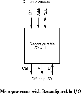
Figure shows a scenario where the off-chip i/o is
completely subsumed by reconfigurable logic. Note that the relatively
low-bandwidth associated with off-chip communications, compared to
on-chip communication, can partially compensate for the slower native
performance of reconfigurable logic. The datapath between the fixed
processing core and the reconfigurable logic can be large, allowing the
reconfigurable logic to use parallelism to achieve reasonable off-chip i/o
bandwidth.
Further, the performance hit due to reconfigurable logic may often be lower
than the performance hit taken when external logic components must be
inserted into the datapath to adapt the processor's i/o to a particular
system.
Similarly, one might worry that the reconfigurable structure will take more
die area than the non-reconfigurable i/o. While the reconfigurable i/o may
be larger, the increase in system cost which comes from having a
larger die may well be less than the increase in system cost which comes
from adding an external IC to adapt the conventional processor to fit into
a particular system.
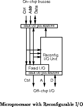
Of course, if one has a favorite bus to support, one could combine the
previous two configurations (See Figure ). Placing
multiplexors both on the i/o pins themselves and the internal datapath
allows the prefered bus to suffer very minimal speed degradation while
allowing full reconfigurability of the i/o interface. This might be
interesting, for example, in building a single IC to span a large range of
systems. The fixed bus structure might be tuned to the highest end product
line. The lower end models could employ the reconfigurable logic to adapt
the core to their systems. This configuration would be particularly ideal
if the lower end systems were cheaper particularly because they ran the
external busses at a lower speed than the high end models.
Application
The variants which allow control over the external interface can be
employed to:
- Adapt to the trendy standards -- Standard bus lifetimes are
shortening and market windows are tight. Currently, if you are going to
integrate native support for some standard bus on your processor (
e.g. PCI, VESA-VL, MBUS), you have to predict the market during CPU design
(12-18 months before product launch). If you guess wrong, you run the risk
of losing out on important design-ins. Additionally, your processor's
lifetime may end up being truncated by the next trendy standard.
Reconfigurable i/o allows you to adapt to popular standards. It might also
allow a system designer the ability to build one card or mother board which
is soft configured for the bus of choice.
- Adapt to non-standard system architectures -- In the
present setting, one cannot get native bus support for busses which lack
widespread industry popularity. With reconfigurable i/o, the processor can
be adapted for direct connection to any bus system. This may be
particularly useful in mixed processor environments and in legacy
system and application environments.
- Adapt to particular memory and i/o configurations --
A reconfigurable i/o interface can be tuned to the characteristics of a
particular system configuration. Block and burst transfer size, block
alignment, timing, and translation can be adapted to the system
configuration rather than being generic. This may allow the system to
naturally accommodate burst transfer modes available from memories or
peripherals rather than being limited by the processor's preconceived and
hardwired block transfer modes.
- Handle low-level protocol processing -- In addition to bus
protocols, the i/o system can be adapted to handle some of the low-level
details of i/o stream processing, particularly those which are best done
with efficient support for bit operations. Stripping off protocol headers,
extracting fields, and responding rapidly to various signaling conditions
are all tasks which can be handled well with flexible hardware.
- Buffer input/output data -- Reconfigurable i/o logic can be
arranged to strategicly buffer data, perhaps according to application or
peripheral requirements, coming and going from the processor. The logic
can provide FIFO buffering as may be useful when embedding a compute
processor in a system. The buffering can be system specific, tuned to the
devices with which the processor is communicating. It can also be
application specific, providing buffering which is appropriate only for
certain kinds of data.
For instance, the processor could pump out program locations for profiling
operations. The reconfigurable logic could take the location data,
timestamp it, then buffer it for a free bus cycle on which to write the
data into memory, and supply the appropriate addresses to store the
profiling data in FIFO style into an allocated region of main memory. Note
that this allows the system to take a time-stamped program trace while only
requiring the processor to execute a store instruction. Since the
reconfigurable logic is doing buffering and translation on-chip, the store
need take no more processor cycles than a store to the on-chip cache.
- Provide direct network interfacing -- The reconfigurable
logic can be used to provide direct interfacing to an attached long-
or short-haul network. This would be particularly useful to adapt
commodity processors for use in large-scale, multiprocessor computing
systems. In the Cray T3D, for example, a separate ASIC is used to couple
an Alpha microprocessor into the high-speed mesh network
[Cra95].
With reconfigurable i/o, the network interface, or a good
portion of it, can be built on chip. This close coupling can provide
much higher network i/o performance, avoiding the overhead of going out to
a remote device over a standard bus in order to communicate with the
network. A network interface is, of course, one place where i/o data
buffering may be necessary.
- Support a variety of peripherals directly -- The
reconfigurable i/o can be used to directly interface peripherals to the
processor, without requiring off-chip glue logic. Chip selects and
peripheral specific timing and control signals can be generated directly by
the reconfigurable i/o. Eliminating glue logic will reduce part count and
system cost.
- Integrate special i/o signaling -- With reconfigurable i/o,
the processor can be configured to handle external events smoothly and
rapidly and provide special output signals. For example, in a polled
device situation, busy or ready signals can be run straight into the
processor's reconfigurable logic. The impact of polling on processor cycle
time need be no more than an on-chip cache access - less, if the signal
can be computed into the processor's branch and conditioning logic.
Similarly, reconfigurable logic can provide special output signals, such as
the context ID in the April/Sparcle microprocessor [ALKK90], the
current priority level, or the process or thread ID of the current running
process.
- ECC or Parity Checking -- The reconfigurable i/o can be
configured to perform ECC or parity computations on data coming and going
from memory in systems where error checking and correction is warranted.
- Reliable Systems Interfacing -- The reconfigurable i/o can be
used to do combining, checking, and voting when building highly reliable
systems. In this setting, the standard microprocessor with reconfigurable
i/o can be adapted to work in such tandem configurations. For example,
in a dual checking system, one can be configured to provide outputs, while
the other can be configured to listen and compare its internal results to
the results of the master. If they ever differ, the backup processor can
signal the main to stop. Again, this reduces system cost by obviating the
need for separate logic components to do the combining and checking.
Additionally, it makes the single microprocessor design with reconfigurable
i/o attractive for use when building reliable systems.
- Synchronization Management -- System specific synchronization
can be handled by the reconfigurable i/o logic. With hooks out to the
actual i/o pins, the processor can generate and receive synchronization
signals directly. The reconfigurable logic inside the processor can
process the signaling accordingly. This could, for instance, be used to
implement barrier synchronization in a multiprocessor. More interestingly,
perhaps, it would allow one to implement application specific
synchronization schemes. In some cases local synchronization between a
few processors may be all that is required for correctness, and the
reconfigurable processors can be adapted accordingly.
With the reconfigurable logic optionally in the i/o datapath, the
flexible logic can be used for:
- Byte swapping -- When the native byte order for the
processor differs from that of the data being handled, the reconfigurable
logic can provide the byte reordering as needed. Examples of cases where
selective byte swapping may be necessary include attached peripherals or
coprocessors with different byte orders, system or network software which
expects a particular byte order, or file formats which require a specific
byte order.
- Field extraction and insertion -- When formatting or
processing messages, protocols, or packed data, the processor may need to
selectively extract and rearrange fields for processing or storage.
- Encoding and Decoding -- Often a data stream must be decoded
before processing or encoded before exiting the processor. The
reconfigurable logic can serve to translate data appropriately for internal
use. Common examples include de/encryption of data for secure storage and
transmission and (de)compression to minimize storage space or transmission
time.
- Scatter/gather addressing -- Often the processor's i/o
system needs to remap addresses in some systematic way to address a
data structure efficiently. For example, in the Cray T3D, an external
address unit remaps addresses to block and distribute array elements
[Cra95]. The
reconfigurable i/o can be programmed to remap the addresses in an
appropriate, data structure and system specific manner.
Advantage Summary
Generally, we can summarize a few common advantages for a reconfigurable
i/o interface:
- Performance -- Direct, on-chip interfacing saves the
requisite chip-crossing latency associated with interfacing the
processor to a peripheral or system using a separate ASIC.
- Costs -- System costs are reduced by reducing the number and
kind of components required to interface the processor to its
peripherals and system environment.
- Flexibility -- The reconfigurable i/o processor can adapt
rapidly to changing and varied system architectures and standards
and can serve to differentiate products.
Attached Logic or Function Unit
Another important application for processor-coupled reconfigurable
logic is to serve as an application specific accelerator. Here, we use the
reconfigurable logic to build logical functions and operations which are
used heavily by a particular application. To achieve low-latency and
high-bandwidth between the processor and the reconfigurable logic, we
attach the reconfigurable logic directly to the processor's register file
along with the fixed functional units ( e.g. ALU, IU, FPU, LD/ST,
MDU).
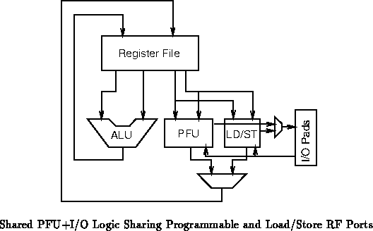
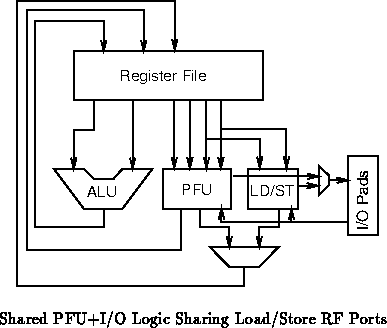
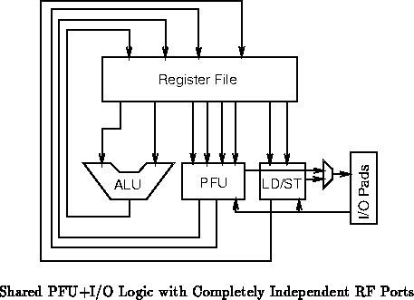
Architectural Options
Recall our basic microprocessor organization from
Figure . When we focus in on the interface between the
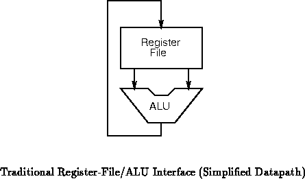
register-file and ALU, the typical organization looks like
Figure . Here, a two read, one write port register
file is coupled to a single ALU. Register-file addresses are generally
derived from the decoded instruction stream and are not shown in
Figure .
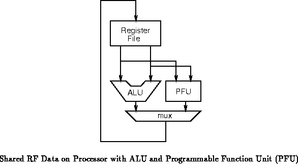
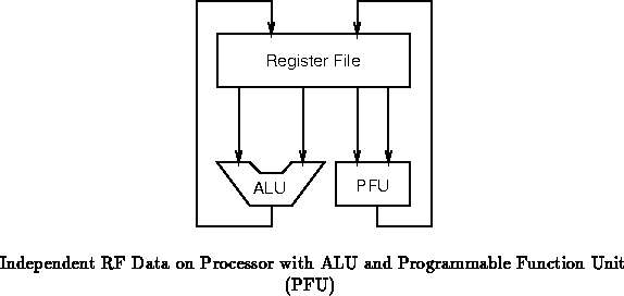
Figures
and show two simple options for the
addition of a single programmable function unit (PFU) to the traditional
RF/ALU organization shown in Figure . In
Figure , the RF ports are shared between the
ALU and PFU allowing the processor to retire at most one result from each
functional unit on each cycle and allowing at most two operands to be sent
to the ALU/PFU combination each cycle.
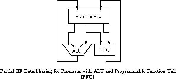
Figure has independent read and write
ports allowing both to operate independently and fully in parallel. Of
course, hybrids between these two extremes are also possible ( e.g.
Figure , which shares one of three read ports between
the ALU and PFU). Reducing the number of read/write ports into the
register file, allows the register file implementation to be simpler and
faster, while increasing the number of ports allows a larger range of
operations to occur in parallel.
Today's high-end microprocessors, generally have multiple, fixed
functional units, exploiting parallelism to increase throughput. In these
superscalar and VLIW configurations, the programmable function unit (PFU)
would take its place alongside the fixed function units.
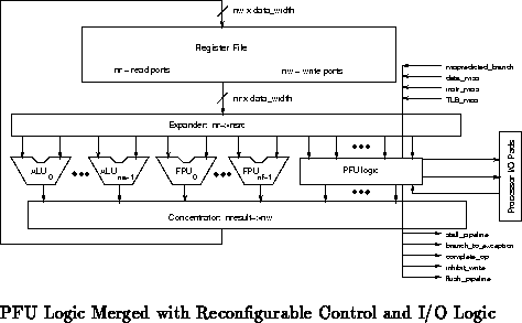
Figure shows the general organization of the
processing core of such a superscalar or VLIW processor. The expander and
concentrator blocks abstract away the large range of datapath sharing which
could go into an implementation. As with the simpler examples above
(Figures , ,
and ), the number of register file ports can
be conserved by sharing them among functional units at the expense of
restricting the options for parallel operation.
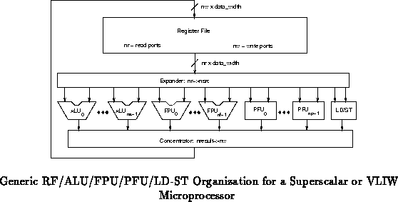
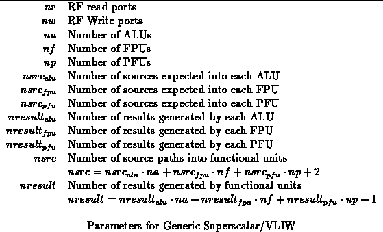
Table summarizes the parameters included in the register
file and fixed unit datapath shown in Figure .
This assumes a single load/store unit taking in a single address-data pair
and generating a single data result. Of course, multiple load store units
with varying input/output interfaces are also possible.
Note, as long as  , read port sharing will be necessary in the
expander. Similarly, as long as
, read port sharing will be necessary in the
expander. Similarly, as long as  , write port sharing will be
necessary in the concentrator.
, write port sharing will be
necessary in the concentrator.
It is also worth noting that it is generally better to share the logic
among PFUs. Consequently, rather than designing the processor with  independent PFUs, one would design on large PFU, perhaps times as
large as a typical single PFU, and provide it with
independent PFUs, one would design on large PFU, perhaps times as
large as a typical single PFU, and provide it with  and
and  inputs and outputs. This also give the PFU set additional flexibility in
utilizing its RF read and write bandwidth.
Figure shows this configuration.
inputs and outputs. This also give the PFU set additional flexibility in
utilizing its RF read and write bandwidth.
Figure shows this configuration.
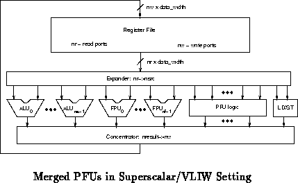
Similarly, in designs where flexible i/o is also desirable, as described in
Section , it may be beneficial to merge the PFU
reconfigurable logic with the input/output reconfigurable logic.
Figure shows a case where the load/store
function is subsumed by reconfigurable logic (compare
Figure ). Figure shows
the analog to Figure , where the fixed load/store and
programmable logic exist in parallel.
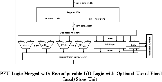
Figures through show specific, small
examples with a single ALU, a single PFU unit which can serve as
reconfigurable i/o, and a single hardwired load/store unit. The primary
difference among these examples is the number of RF read/write ports and
hence the function of the expander and concentrators.
Timing Control
Assuming the processor runs at some fixed rate
independent of the
function implemented in the PFU, the logic coupling may have to deal with
various timings which are possible in the PFU.
- Single cycle latency, Single cycle throughput -- In the simplest
case the PFU function may operate within the standard pipeline clock
period of the processor.
- Multiple cycle latency, No new Operations while Operation in
Progress -- In some cases the latency of the PFU operation may be multiple
clock cycles. In the simplest multiple cycle case, the processor will not be
able to issue a new operation until the previous operation completes.
- Multiple cycle latency, Single cycle throughput -- If the
programmed function is pipelined, the processor may still be able to issue
a new operation every cycle.
-
 -cycle Latency, Launch every
  -cycles -- In the general case,
the processor may be able to launch a new operation every cycles, while
the operation completes cycles after launched.
-cycles -- In the general case,
the processor may be able to launch a new operation every cycles, while
the operation completes cycles after launched.
- Multiple Latency Function -- Sometimes a PFU may implement several
functions with differing, but predictable latencies.
- Variable Latency -- Some operations may have data dependent
latencies.
We can handle most of these cases in the same way analogous cases
are already handled in processors. The main difference being that fixed
functional units fall into one of the categories which is known at design
time, whereas the category here will depend on the function being
implemented and hence will not be known until the function is configured.
Predictable delay constraints can be scheduled in software. That is, the
compiler can guarantee to only emit code which will launch a new operation
every cycles and expects the result of an operation to only be
available after cycles. The compiler will know the PFU function when
generating the code to accompany it, so can arrange code appropriately to
handle the specifics of a particular PFU.
To support variable times, the control logic can accommodate
ready and busy signals from the programmable logic. The PFU can, for
instance, have a pair of extra signals, one to indicate when the result is
done and one to indicate when the PFU is ready for the next operation.
These control signals would be generated from the programmable logic and be
customized to each PFU configuration. The controller can then stall the
pipeline when the PFU is not ready for input. Similarly, it can use the
result completion signal to determine when to writeback the result and when to
stall dependent computation. The processor could, for example, use a
standard register score-boarding strategy to force the processor to stall
only when the instruction stream attempts to access the PFU result before
it is generated.
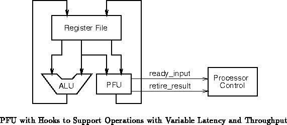
Figure shows such an arrangement. ready_input is
asserted whenever the PFU is ready to receive a new input.
retire_result is asserted when the PFU completes each operation. The
processor control will stall the pipeline if ready_input is not
asserted when the next operation in the pipeline requires the PFU. The
processor control uses retire_result to recognize when a result is
done and make sure writeback occurs to the appropriate target register at
that time. When the PFU instruction is issued, the result register is
marked unavailable. If the processor control encounters any reads to
unavailable registers, it can stall the dependent instruction awaiting the
writeback which makes the value available.
Of course, a particular processor could choose to restrict the
kinds of variability allowed to simplify control. Implementations could
restrict themselves to no variability or to variability only in launch rate
or completion latency.
Diverting Control Flow
Other hooks into the processor's control flow may be merited. In
particular, there are a number of applications where it would be beneficial
to give the logic an option to divert program flow rather than simply stall
it. Two general classes:
- Exception/assumption detection -- The processor code could be
compiled assuming certain cases do not occur. The PFU could then be
programmed to watch values and detect when these exceptional cases occur,
diverting the processor's control to handle the exceptional case
accordingly. For example, compiled code could be written assume a certain
address rage is never written, allowing the values to be cached in
registers or even compiled into the code. The PFU then performs parallel
checking to see that this assumption is met throughout the region of code.
In a similar manner, the PFU might be programmed to watch for specific
address writes to facilitate debugging.
- PFU limitations -- Similarly, the PFU may implement a restricted
version of some function -- perhaps one that only works for certain values.
When unusual values, those not handled by the PFU, are detected the PFU
could divert control flow to software which implements the function.
As described, this could simply be a line which signaled a synchronous
exception vectored into a handler setup to handle the specified exceptional
event. Alternately, the line could set dirty bits in the processor state,
thread state, result registers, or the like to indicate that the computed
value was incorrect and should be ignored. Such a line might also inhibit
memory writes or other side-effecting operations which might write
incorrect results based on the violated assumptions.
Control Registers
In some cases it may be useful to place
specialized control registers inside the PFU. For example, for a DPGA PFU
it might be beneficial to have a dedicated context state register for the
array inside the PFU. This would be particularly advantageous if the PFU
performed multiple cycle functions in the same PFU, but the processor did
not want to allocate register file or instruction bandwidth to feed the
context identification into the PFU on every cycle. Some internal
registers may be beneficial anytime when the PFU operates on logical input
data larger than its register file datapath. Internal registers can always
be built out of the programmable logic, but where we can anticipate their
common need, it is cheaper to go ahead and include fixed registers.
Control Inputs
So far, we have described scenarios
where the PFU simply takes data from the register file datapath. We may
want a control signal into the PFU indicating when new data is valid and
destined for the PFU. Of course, if the PFU can always operate on the data
its provided and the processor only takes results from the PFU when it
expects the PFU to generate results, such control is not strictly required.
However, if the PFU is tied up for multiple cycles with each operation, as
suggested in some usage scenarios above, the PFU needs to be told when it
actually needs to start operating on data. Additional control signals
might tell the PFU more about what to do. For example, if a PFU is setup
to perform more than one operation, the PFU might get some instruction bits
to specify the current operation. Similarly, control bits might inform the
PFU about the kind of data it is now receiving via its register file
inputs. This information would be particularly valuable if the PFU
operated on more data than it got over the register file datapath in a
single cycle and did not always get all of the data it operates on reloaded
in a deterministic sequence.
Orchestrated DPGA/SIMD Logic
We can also view the processor
sequencing and control as an orchestrator, coordinating DPGA or SIMD
logical operations occuring within the PFU. This view is entirely
consistent with the general scheme presented here. A processor designed
specificly with this in mind is likely to include more PFU logic and less
fixed ALUs. In fact, the fixed ALUs might exist primarily for addressing,
control branching, exception handling, and configuration loading.
Application
- Special Purpose Functional Units -- The primary application
for the programmable functional unit model is, of course, as special
purpose functional units adapted to a particular application. Operations
which are executed frequently in the application, but poorly supported in
the fixed processing units, can be implemented in the PFU to accelerate the
application.
- Matching, Searching, and Filter -- One class of
operations for the specialized functional unit is to support efficient data
filtering. When the processor needs to process large amounts of data
looking for certain characteristics, the PFU can be programmed to identify
the desired characteristics allowing the processor to rapidly walk over
large datasets. This kind of support is likely to be valuable in database
and transaction processing applications.
- Exception/assumption checking -- As noted above, the PFU can
also be used for assumption checking and error detection in support of
speculative and common-case execution on the fixed or programmable
functional units.
- Fine-grained Parallelism -- PFUs implemented with
fine-grained logic ( e.g. FPGAs or DPGAs) can very efficiently
take advantage of fine-grained, application-specific parallelism. This
kind of parallelism is handled particular poorly with traditional, fixed,
wide ALUs.
- Special Purpose State Collection and Computation -- State can
also be built up inside the PFU. The PFU can thus be used to maintain
specialized state adapted to a particular application. Further, the PFU
can implement logic to efficiently update that state as new data is
collected or events occur. For example, the PFU could implement a
pseudo-random number generator, maintaining the pattern state internally
as well as computing functional updates. A wide range of statistics
collection could be implemented this way. The processor could fire data
values at the PFU, and the PFU would use the new data to update its
statistical residues to be retrieved by the processor once the monitoring
period ends.
Advantage Summary
- Performance -- The programmable functional unit arrangement is
primarily aimed at increasing the performance of the processor by allowing
the inclusion of application specific acceleration logic.
- Functional Extension -- This coupling makes some operations
feasible which are conventionally infeasible. Operation and value
checking can support debugging. Lightweight data collection and
maintenance can facilitate minimally intrusive profiling and
monitoring.
Control Logic
An interesting class of reconfiguration becomes available when
reconfigurable logic is interfaced with the basic control circuitry for the
processor. In the previous section we began to introduce some special cases
where allowing the reconfigurable logic direct access to consume and
generate control signals will expand the range of adaptation possible. In
this section, we focus more specificly on this class of reconfiguration
which is useful apart from its coupling to PFU logic.
Architecture
Every traditional microprocessor has logic which controls the flow of
instructions and data. This logic usually accounts for a very small
portion of the silicon area on the processor die, but plays a large role in
establishing how the processor behaves and what it does efficiently.
Direct hooks into this logic allow us to reconfigure the basic processor
behavior. The hooks could range from allowing reconfigurable logic to
drive into selective fixed-logic signals, as suggested for the stall in the
previous section, to replacing the fixed control logic with a
reprogrammable substrate. The latter offers more flexibility while the
former allows faster and smaller implementation of standard control
structures. Just like the flexible input logic, default, hardwired control
logic can be wired in parallel with reconfigurable logic to give some
elements of both schemes.
In general, reconfigurable logic might monitor:
- various data and address lines on the chip -- The logic may use
these inputs to detect unusual events or assumption violations.
- cache miss, conflict, TLB miss lines, read/write control lines,
processor stall, pipeline flush, branching, branch prediction, mispredicted
branch -- Access to these signals will be particularly useful when the
reconfigurable logic controls behavior in exceptional cases like, cache or
TLB misses.
- i/o's -- As noted in Section , direct access to
the i/o's is beneficial in adapting the processor to a system and
the devices it is operating with. This kind of access on some i/o
signals is useful for adapting control and signaling even if the
primary i/o busses are not reconfigurable.
All of these lines can be monitor for profiling, debugging, and
statistical purposes.
The reconfigurable logic might control:
- processor stall, pipeline flush
- next instruction
- read/write control (internal writeback and external)
- outputs
This kind of control was introduced in Sections
and , and is also useful independent of a programmable functional
unit or reconfigurable i/o.
When reconfigurable control logic is arranged in this manner, the
processor's behavioral patterns can be revised. In some cases, this may
allow the reconfigurable logic to control what happens on exceptional
events like traps, cache misses, TLB misses, or context switches. It may
also allow the instruction stream to make more or less stringent
assumptions about the data and provide a means of checking these
assumptions and handling the data accordingly.
Among other things, this may allow the processor to be adapted to match
the semantics desired by a particular operating system or operating
environment. In many modern systems, the OS ends up executing many
instructions to switch contexts, take traps, or save/restore registers
because the processor does not quite provide the right hooks to match the
OS semantics ( e.g. [ALBL91]).
Reconfigurable control can provide an opportunity to make up for semantic
gap at the processor level, rather than incurring large software overheads
to emulate the desired semantics.
In general, the control logic on the processor is the hardest part
to get correct. The various exceptional and hazard cases, and their
interactions, are difficult to handle well and correctly. Sometimes it is
difficult to decide what the correct behavior should be. With highly
reconfigurable control logic, we defer the binding time, allowing the logic
to be fixed after the processor is fabricated and allowing the behavior to
be revised without spinning a new design.
If one does combine reconfigurable control with a programmable
functional unit (Section ) or reconfigurable i/o
(Section ), it may make sense to combine the
reconfigurable logic into one large block. This allows sharing and
averaging. When the control is simpler, more space is available for i/o or
programmable functions. Similarly, when the control is large, it can
borrow space from the other reconfigurable units.
Figure shows our basic processor datapath
with a reconfigurable logic block serving as a PFU, reconfigurable i/o, and
which includes hooks into the processor's control logic.
Application and Advantage Summary
- Behavior Modification -- The processor's behavior can be
modified, allowing it to be tuned for the characteristics of a particular
application or adapted to provide particular semantics.
- Profiling and Monitoring -- Direct hooks allowing
reconfigurable hardware to monitor on-chip signals supports a wide variety
of low-overhead profiling which is currently impossible. Key, on-chip,
lines and datapaths can be monitored with event computation and handling
processed directly in reconfigurable logic. Simple statistical gathering
can update state in the reconfigurable logic without perturbing processor
operation. Coupled with sufficient hooks into the i/o, the logic may even
be able to store events off to memory without interrupting the processor's
execution. More elaborate schemes can use the reconfigurable logic to
detect events then divert program flow to allow the processor to run code
to further handle the event.
- Debugging -- Combining control of processor flow with event
monitoring, the reconfigurable logic can be used to provide rich debugging
support. Breakpoints can be set based on internal processor state.
Customized action can even be defined to snapshot and preserve precious
state when targeted events occur.
- Exploit on-chip bandwidth -- On chip access to internal
signals and is moderately inexpensive. However, limitations in off chip
bandwidth make it impractical to route internal signals off chip for
observation or control. On-chip reconfigurable logic makes it possible to
access these signals economically.
Instruction Interpretation
The processor reads the instruction from the cache and controls
execution accordingly. In modern, RISC microprocessors, the instruction is
decoded by hardwired control logic to manipulate each stage of the
processor's pipeline. Reconfigurable logic can be integrated into the
processor's instruction stream decoding in a number of ways:
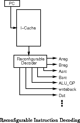
- Straight -- the reconfigurable logic interprets the instruction
stream, controlling the code, effectively taking the place of the
fixed decoder and control (See Figure ).
- Microcode-like -- the reconfigurable logic can turn the
instruction into a sequence of primitive operations and control
their flow through the processor. This is much like traditional
microcode, except that the control is implemented in the
reconfigurable logic rather than a microcode PROM.
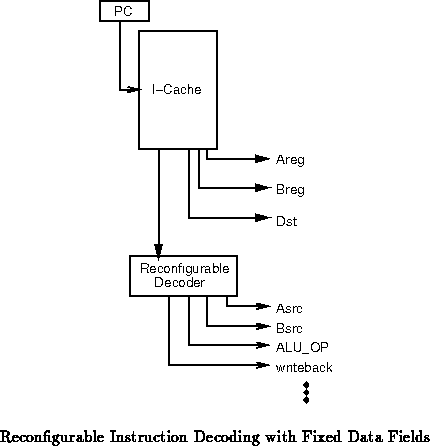
- Fixed/Flexible Hybrid -- A hybrid flexible/hardwired scheme, might
provide direct paths for common operands such as register file
addresses, while the reconfigurable logic has complete control over
operation interpretation and control signals (See
Figure ).
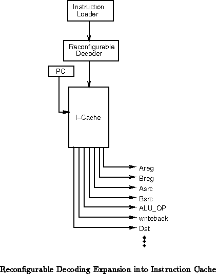
- Code Expansion -- the code can also be expanded from a denser,
memory efficient form, into a larger, more workable form when stored in the
I-cache ( e.g. CRISP [DMB87]). The instructions returned from
the I-cache are thus expanded instructions which directly control the
on chip resources. In some ways this is reminiscent of the decoding which
can be applied to data on the processor's input datapath when using
reconfigurable i/o (Section ). Of course, this
configuration has a straight and hybrid scheme, as well.
Figure , shows the straight version.
Application and Advantage Summary
- Decode and emulate instructions -- Flexible instruction
interpretation allows the processor to be adapted to efficiently
decode and run instructions for some fixed processor. The flexible
logic decodes the provided instruction stream and reformulates them
into the control structures on this processor. In general, this may
require expanding some instructions into multiple operations on the
core processor.
- Customize instruction stream to application -- The
instructions can be customized to the application. This can be used
to compress executables by adapting the instruction encoding to the
application instruction usage. As a simple example, we could derive the
optimal Huffman source coding for a binary, then revise the
instruction encoding accordingly. Of course, more sophisticated
recodings will provide greater benefits.
- Ease incorporation of configurable structures -- Customized
instruction decoding is complimentary with the other reconfigurable
structures introduced here, allowing us to adapt the instruction stream to
directly accommodate new instructions and behaviors made possible by the
reconfigurable logic.
Basic processor behavior
Architecture
A classic question in processor architecture is: ``where should resource
be deployed.'' Should the cache be larger/smaller relative to the TLB?
Do we allocate space to prefetch or writeback buffers? How much memory
should go into the data cache, instruction cache, scratchpad memory? Do we
include a branch target buffer or victim cache?
A second question which comes along with this one is: ``How do we manage
the limited resources?'' What's the prefetch/reload/eviction policy?
The traditional solution to both of these questions is to make a
static decision at design time which does, in some sense, reasonable well
across the benchmarks the designers consider representative. This
inevitably leads to compromise for everything, and for many applications
the magnitude of the compromise can be quite large.
With a reconfigurable processor we can, instead, leave some
flexibility in the architecture so the machine can be configured to deploy
the resources most effectively for the given application. The idea is to
go ahead and build specialized pieces of hardwired logic with common
utility ( e.g. memories, ALUs, FPUs), but rather than completely
hardwiring their control and datapaths, leaving flexibility to reorganize
their interconnect and hence use.
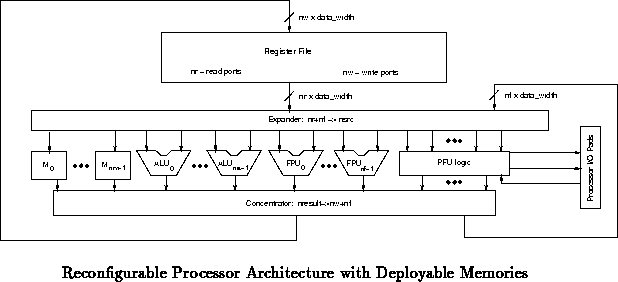
Figure , for example, shows a revision of our
generic VLIW processor architecture where blocks of configurable memory
have been added to the collection of processing resources. Here, some
outputs from the ALU/PFU/FPU/memory bank are routed back to the expander to
allow cascaded operations. For example, a virtual memory address coming
out of a register may be translated through a memory before being
feed to the i/o. Similarly a base address from one register may be added
to an index from another before the address is fed in as an address to the
the cache. To facilitate this, we conceptually add  additional outputs
from the concentrator and
additional outputs
from the concentrator and  inputs to the expander, in addition to the
additional concentrator inputs and expander outputs entailed by the
additional memory units they support.
inputs to the expander, in addition to the
additional concentrator inputs and expander outputs entailed by the
additional memory units they support.
Additionally, the memories can be arrange in standard sized chunks which
can be composed, allowing the memory resources to be shuffled at a moderate
granularity. For example, each basic memory could be a 2Kx8 memory chunk.
4 or 8 of these can be grouped together to build a 32- or 64-bit wide
memory. Additionally, they can be cascaded to build deeper memories. So,
 could be cascaded to build an 8Kx32 memory.
With a little bit of additional control logic, these memories can be used
as caches, cache-tags, TLBs, explicit scratchpad memories, FIFO buffers, or
the like. These memories can completely subsume the separate data cache
shown in our original processor model (Figure ). The
additional control logic is likely to be supported largely in
reconfigurable logic as suggested in Section .
Systems that do not use a TLB can reallocate memory blocks to the cache.
Applications with more or less virtual memory locality can adjust the size
of the TLB accordingly. Applications with known data access, can use
explicit scratchpad memory, reallocating the memory blocks holding cache
tags to data storage. Applications with specific spatial locality in data
or instructions, can build logic to prefetch data according to the
application need.
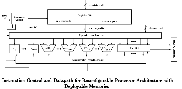
Figure expands the datapath to show the
processor control. In particular, this organization makes it clear that
the instruction cache can be implemented out of the memory units, as well.
Each application can now trade-off memory between the i-cache and d-cache
based on the needs of the application.
We can also view the register file as another memory which can also be
built out of the deployable memory units. Figure
shows a configuration where there is no a priori designated register
file. Rather the register file is built out of the memories. This may
allow, for example, the reconfiguration of the register file width, depth,
and number of simultaneous read ports. Further the register file can be
broken into a series of smaller register files where appropriate.
Here, the expander/concentrator is collapsed into a single reconfigurable
interconnect.
Alternately, the register file may want to be a slightly specialized memory
unit, but still be deployable for the reasons articulated here. As noted
above, width, depth, and read cascading are moderately easily constructed
by paralleling memory blocks just as in building basic memory structures.
What is harder to build by composition is multiple write ports, and
register files often depend heavily on a number of simultaneous write
ports. For this reason, it may make sense to also include a different kind
of memory block with multiple write ports to allow efficient construction
of register files, as well as other structures requiring simultaneous write
support.
The configuration shown in Figure shows hardwired
processor control and a completely reconfigurable i/o unit. Of course,
variations could implement all or much of the control in reconfigurable
logic and/or include hardwired load/store units.
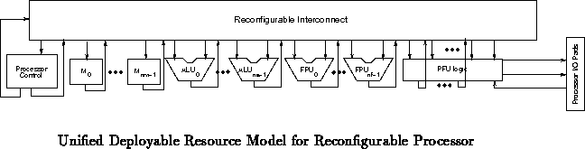
This finally leads to a revised model for a computing device in which
basic, specialized functional units ( e.g. memories, ALUs, FPUs, MDUs,
LD/ST units, DMA logic, hardwired control units) are embedded in a
reconfigurable interconnection scheme along with regions of reconfigurable
logic which can be used for monitoring, control, i/o, decoding, and as
PFUs. This device gains the performance and space advantages of hardwired
logic units for commonly used operations. At the same time, it gains
performance advantage over a purely fixed microprocessor by adapting the
processor organization much more tightly to the application.
Note that the reconfigurable interconnect used to interconnect functional
units differs both from the fine-grained reconfigurable interconnect
typically employed in FPGAs and the expander/concentrator interconnect used
in a pure VLIW. Rather, it is a hybrid of the two. Unlike traditional
FPGA interconnect, most of the operations with the interconnect are bus
oriented. Therefore, busses are switched in groups. Most busses may be
some nominal processor bus width ( e.g. 16, 32, 64). Some will be
able to compose or decompose these busses to other interesting sizes (
e.g. 1-bit entities for fine-grained logic, 8-bit entities for
reconfigurable memories). In a traditional VLIW, the decoding of the
instruction specifies the configuration of busses. With this kind of a
setup, the instruction bandwidth would be excessive if fully configured
from the instruction stream. Similarly, the interconnect pattern would be
too rigid if fully configured via FPGA style programming. Here, the
configuration of busses will depend partially on the instruction executed
and partially on the way the system is currently configured. In most
scenarios the decoding between the instruction stream specification of
interconnect and the full interconnect specification would be done in the
reconfigurable logic. For efficiency, the reconfigurable logic serving
this purpose might be tailored somewhat to this application.
Application and Advantage Summary
- Deploy resources where needed -- As noted, limited resources
can be deployed where they most benefit the application or system using the
processor rather than being statically deployed according to aggregate
statistics across all applications and systems.
- Arrange datapaths as needed -- Datapaths can be organized to
match the application requirements. For example, ALUs and register ports
can be cascaded to operate on wider data efficiently. Also, data can flow
directly from one functional unit to another without an intervening store
into and read from the register file.
- Systolic operations -- Perhaps as a special, well
understood, case of application-specific datapath and resource arrangement,
systolic arrays or pipelines of functional units can be arranged allowing
data to flow through standard sequences of operations and adapting
the processor to exploit task-specific parallelism.
- Structure parallelism to the problem -- In general,
deployable functional resources allow the processor to structure the
parallel operations in accordance with the application. Applications with
high, static parallelism can schedule resources staticly for parallel
operation. Applications suitable to pipelined parallelism can be organized
in that manner. Applications with heavy dynamic dependencies can allocate
part of the resources to detecting conditions under which serialization is
necessary.
- Adapt management strategies to application characteristics --
With the addition of reconfigurable control, resources management
characteristics can be tuned to the application.
Reconfigurable Logic
The reconfigurable logic can be realized as one of many different
structures.
- FPGA -- Traditional, fine-grained logic modules with
programmable interconnect ( e.g. Xilinx LCA [Xil93]) is one
likely candidate. The fine-grained structure is particularly good for
random logic and bit manipulation.
- DPGA -- Multiple context programmable logic ( e.g. DPGAs
(tn95)) can provide density advantages over more traditional
FPGAs, especially in situations where well defined subsets of the
logic operate at different times. DPGAs also allow non-destructive
background loading which can help reduce effective configuration
overhead.
- PAL -- PAL-like array structures are good for smaller blocks
of logic or for fast decoding.
- Memory -- In some setting a block of memory can serve as an
efficient, programmable translation resource. Most
programmable technologies are implemented out of smaller memories
with programmable interconnect.
- MATRIX or other reconfigurable datapath array architecture --
MATRIX is a more coarse-grained, datapath oriented
architecture which has more specialized memory and ALU primitives
and operates on multi-bit bussed data. Similarly, Wang and
Gulak's
reconfigurable datapath array architecture [WG94]
provides more coarse-grained, datapath oriented, reconfigurable
blocks suitable for building a microprocessor datapath.
These architectures represents a configurable design point somewhere
between a fixed processor and a bit-configurable
FPGA. In many ways a MATRIX array is an
extreme of the deployable fixed-unit organization described in
Section . As such, MATRIX may be well
suited for certain classes of PFU implementations.
- MATRIX/DPGA Hybrid -- In practice, a mix of fine-grained
control and more specialized functional units embedded in a common
reconfigurable mesh may be a very attractive choice for the
the reconfigurable logic in PFU and i/o logic.
Much of the logic used in the i/o path and, to some extent, in the
PFUs, is likely to be datapath oriented. Consequently, it will probably
make sense to specialize a good portion of the array logic to datapath
usage. This datapath specialization may include routing busses, slaving
multiple programmable cells off of a single configuration ( e.g.
[CL94]), and including bussed register banks. The
benefit of datapath orientation is greater density and performance on
datapath applications than regular FPGA/DPGA structures. Fine-grained
logic will still be desirable for control operations and bit-wise
manipulations.
Configuration Reloading
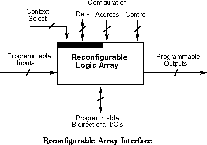
Figure shows the generic, logical view
for a reconfigurable array. The programmable i/o's are shown separate from
the configuration facilities.
The configuration i/o's control the loading of the array's configuration or
context. The configuration port can look very much like a memory port.
Depending on the design requirements, the port can be anything from a 1-bit
serial data port with no address control to a 64-bit wide (or larger) data
port with full, random access address control to the internal configuration
memories. Wider datapaths support more rapid context loading.
Random access to the configured logic allows rapid, incremental changes in the
array personality.
The programmable i/o's are inputs to the logic implemented in the
reconfigurable array and outputs generated by the array. There need be
little direct correspondence between the number of i/o's and the size of
the array. In some situations, it will be beneficial for all i/o's to be
bidirectional i/o's -- e.g. if the array is being coupled to a common
bus on the processor. More likely, in processor-coupled applications, it
will be beneficial for all the i/o's to be dedicated inputs and outputs.
For multicontext ( e.g. DPGA) designs, a context select will specify
the active context. This may come from a special purpose register driving
the context select, from hardwired logic, from decoded CPU signals, from a
hardwired sequencer, or even from a programmable output from this or
another reconfigurable logic array.
In a processor-coupled scenario, we could place the reconfiguration loading
data and address path in any of several places:
- Register File Port -- We could couple the reconfiguration
data and address path into the register file datapath, perhaps even sharing
the ports into the reconfigurable unit used as a programmable PFU or
reconfigurable i/o. This allows high reload bandwidth, but also requires a
processor cycle for each configuration word transfered into the
reconfigurable control unit.
- Shared I/O Path -- Alternately, we could wire the configuration
port into the i/o path. This would allow configurations to be loaded
directly from memory without being first loaded into the register file.
This could still require processor direction to control the loading of
data. If a separate DMA unit is available on the processor, the processor
could start a DMA transfer to load a new configuration from memory,
then go about computing in parallel with the configuration load.
- Separate I/O Path -- A separate i/o path could be provided
for reconfiguration. This path might go to dedicated configuration memory.
In this case, DMA i/o would be most sensible, since the separate path
allows configuration to take place without interrupting processor
load/store/fetch operations. This options is, of course, more costly and
less flexible than those which share the processor's i/o path and main
memory for configuration loading and storage.
See Also...
References
- ALBL91
-
Thomas Anderson, Henry Levy, Brian Bershad, and Edward Lazowska.
The Interaction of Architectures and Operating System Design.
In Fourth International Conference on Architectural Support for
Programming Languages, pages 108-120. ACM, April 1991.
- ALKK90
-
Anant Agarwal, Beng-Hong Lim, David Kranz, and John Kubiatowicz.
APRIL: A Processor Architecture for Multiprocessing.
In Proceedings of the 17th International Symposium on Computer
Architecture, pages 104-114. IEEE, May 1990.
- BDK93
-
Michael Bolotski, Andre DeHon, and Thomas F. Knight Jr.
Unifying FPGAs and SIMD Arrays.
Transit Note 95, MIT Artificial Intelligence Laboratory, September
1993.
[tn95 HTML link] [tn95 PS link].
- CL94
-
Don Cherepacha and David Lewis.
A Datapath Oriented Architecture for FPGAs.
In Second International ACM/SIGDA Workshop on Field-Programmable
Gate Arrays. ACM, February 1994.
proceedings not available outside of the workshop, contact author
lewis@eecg.toronto.edu.
- Cra95
-
Cray Research, Inc.
CRAY T3D System Architecture Overview Manual, 1995.
URL
http://www.cray.com/PUBLIC/product-info/mpp/T3D_Architecture_over/T3D.overview.html.
- DeH94
-
Andre DeHon.
DPGA-Coupled Microprocessors: Commodity ICs for the Early 21st
Century.
Transit Note 100, MIT Artificial Intelligence Laboratory, January
1994.
[tn100 HTML link] [tn100 PS link].
- DMB87
-
Dvid Ditzel, Hubert McLellan, and Alan Bernbaum.
The Hardware Architecture of the CRISP Microprocessor.
In 14th International Symposium on Computer Architecture, pages
309-319. ACM/IEEE, IEEE Computer Society Press, June 1987.
- GSH94
-
Greg J. Gent, Scott R. Smith, and Regina L. Haviland.
An FPGA-based Custom Coprocessor for Automatic Image Segmentation
Applications.
In Duncan A. Buell and Kenneth L. Pocek, editors, Proceedings of
the IEEE Workshop on FPGAs for Custom Computing Machines, Los Alamitos,
California, April 1994. IEEE Computer Society, IEEE Computer Society Press.
- HTA94
-
Neil Howard, Andrew Tyrrell, and Nigel Allinson.
FPGA Acceleration of Electronic Design Automation Tasks.
In Will Moore and Wayne Luk, editors, More FPGAs, pages
337-344. Abingdon EE&CS Books, 49 Five Mile Drive, Oxford OX2 8HR, UK,
1994.
- LWP94
-
Wayne Luk, Teddy Wu, and Ian Page.
Hardware-Software Codesign of Multidimensional Programs.
In Duncan A. Buell and Kenneth L. Pocek, editors, Proceedings of
the IEEE Workshop on FPGAs for Custom Computing Machines, Los Alamitos,
California, April 1994. IEEE Computer Society, IEEE Computer Society Press.
- WG94
-
Qiang Wang and P. Glenn Gulak.
An Array Architecture for Reconfigurable Datapaths.
In Will Moore and Wayne Luk, editors, More FPGAs, pages 35-46.
Abingdon EE&CS Books, 49 Five Mile Drive, Oxford OX2 8HR, UK, 1994.
- Xil93
-
Xilinx, Inc., 2100 Logic Drive, San Jose, CA 95124.
The Programmable Logic Data Book, 1993.
Bandwidth Issues for Coupled Reconfigurable Logic
Recent papers begin to show more explicit evidence that the bandwidth
between the conventional processor (and memory) limits the performance
improvement attainable with the reconfigurable compute engine, typically by
an order of magnitude.
- For a Sobel edge detector, Luk notes, that the hardware-assisted
version is, in practice, only 39% faster than the software only
version. He then notes that the communication overhead accounts
for 88% of the time taken. ``If this overhead is not included, the
hardware-assisted design is approximately 13 times faster than the
software version. Furthermore, if the input-output bottleneck can
be eliminated so that the only speed limitation is the critical
path delay, we estimate that a speedup of about 300 times can be
achieved.'' [LWP94]
- [GSH94] also presented evidence that performance is
directly limited by bandwidth between the control processor and the
reconfigurable system. In their talk, they showed that the reconfigurable
system gave roughly a 10x speedup, but was limited by the low bandwidth
interconnect. They suggested that another factor of ten in performance
acceleration could be realized if the bus bandwidth were increased. The
(preliminary?) paper alludes to the issue, but does not spell out the
result as clearly as the talk.
- For Electronic Design Automation (EDA) tasks,
[HTA94] finds only marginal benefits (speedup
factors between 1 and 8) for off-chip, FPGA co-processors.
They find that the bus bandwidth limitation is largely
responsible for this bound.