MBTA: Node Architecture Selection
Andre DeHon
Tom Simon
Original Issue: June 1990
Last Updated: Wed Nov 10 22:51:21 EST 1993

This note summarizes several node architectures which were originally under consideration for MBTA. This may be of interest to anyone wondering why we settled on the node architecture we did. Also, it may be useful to see how the architecture might have differed if our goals were weighted differently.
On one hand, we want to have a generic node architecture capable of allowing fair emulation of many possible node architectures. On the other, we want to be able to test the RN1 based network at full speed to test performance, packaging, cooling, and reliability. Along with these goals, we would like to have a very general architecture which both is simple and small. See (tn17) and [DeH90e] for a more detailed explanation of the goals and purposes of MBTA.

As we attempt to settle on a node configuration for MBTA, it is worthwhile
to consider what the node architecture for a real machine might look like.
Figure shows one possibility for the eventual
architecture of a node in a multiprocessor computer system. Main memory
may or may not support the independent read/write ports shown. The way in
which it supports these ports ( e.g. banked memory, time-sliced
access, multi-ported RAM) is abstracted away for the time being. In this
configuration, most of the time it should be possible to keep the processor
running, make network requests through net-out, and service two
incoming requests through net-in simultaneously.
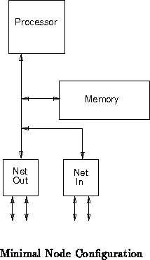
A node with a single bus and processor (Figure ) is the
simplest MBTA node configuration possible. In this case, the single
processor simulates the function of the entire node. No parallel
operations occur on the node. In a single node simulation cycle, the
processor runs a time slice of all hardware that might be on node
Features
Bugs

In order to stand a chance of using and servicing the bandwidth of the
network, the node must be able to support three concurrent operations
between the node and network. Figure shows one configuration
that attempts to meet this goal. The processor simulates the compute
processor and whatever other hardware might be on the node ( e.g.
memory processor). The network processor simply processes network
requests; in particular, it handles the rop operations
described in (tn19) and [DeH90b]. The network processor runs
in a tight loop checking for rop operations from the
network and dispatches to service them accordingly. The memory is
duplicated. This effectively provides the node with two read ports into
memory. Writes, however, require access to both memory busses in order to
guarantee that the memories remain consistent.
In this scheme, it is possible to take advantage of the three simultaneous network ports in a couple of ways as shown below:
Features
Bugs

It is possible to get some of the benefits of the previous scheme with two independent banks of memory. As long as the processors store their instructions in opposite memory banks, instruction fetches will not interfere with each other. In this case write operations do not require all of the node's memory resources. Similarly, atomic operations completely within a single memory bank only require exclusive access to half of the memory system. If the data is not well distributed between the two memories, access to the over-utilized memory bank can bottleneck node operation.
Features
Bugs
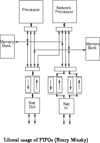
We can expand upon the dual bank configuration using FIFOs to buffer data
coming and going from the node (Figure ). This will allow us to
easily guarantee that transmission and reception can occur at full network
speeds. The FIFOs also gives us buffers to avoid blockage due to critical
resources. Additionally, they make it possible to allow remote operations
to be performed without the full attention of the processor. This should
simplify and the code required to deal with network operations. The FIFOs
will be costly in terms of board area and component expenses. The data and
address bussing, multiplexing, and timing will probably be quite hairy in
this scheme.
At the cost of additional bus and multiplexing hair, it would probably be
possible to use a single FIFO for each pair of FIFO's shown in
Figure . Generally, only a FIFO in a single direction will be
used at once. A single FIFO would be sufficient if the direction of the
FIFO can effectively be reconfigured between operations.

Since Figure may be a bit misleading, a more detailed version of
this option is shown in Figure
. The bus gates shown
deal with arbitration and multiplexing for access to a client bus/device.
Features
Bugs

Figure shows a compromise that, hopefully, satisfies many
of the primary goals of MBTA. This is a simple node configuration with a
single processor and memory. The fast memory is intended to cycle at twice
the rate data arrives from the network. The node is capable of utilizing
full network bandwidth by sending data out through net-out under
processor control while simultaneously receiving data to memory through
both net-in ports. The FIFO associated with the output path through
net-out allows net-out to assume full responsibility for
retrying network operations. The processor only fills the FIFO initially.
Once the network operation is initiated, net-out has all the data
available to retry the operation until it succeeds.
Fair emulation is possible since there is a single stream of execution. The processor simply executes a time slice of each emulated node device during each emulation cycle.
In fast network test mode, the processor feeds write operation over the network and records appropriate statistical information. The write operations are handled directly by the net-in units, leaving the destination node's processor free to be feeding data into the network, also. Periodically, the processor can check the validity of the data written into memory.
When emulating nodes, it would be unfair to run the network at full speed.
The network should only be running at some small fraction of its real speed
to be fairly matched to the simulation. However, it is important in
testing reliability and cooling to be able to run the network at full speed
for long periods of time. To allow these test to coincide with emulation
experiments, net-out and net-in can both send ``dummy'' data to
consume the unused network bandwidth. Rather than running the network
slow, net-out and net-in are designed to service the network at
full speed. However, they do not send simulated data at full speed. They
will send the node generated network data only intermittently. Between
these times, they will send filler data to each other. Both endpoints
agree to only treat every -th byte as network data (where
is a
parameter set at boot time). Between the valid data, the sending node
sends some sequence of random data which the receiving node can anticipate
and verify ( e.g. the sending node could simply send the contents of
a byte wide counter running at network speed). This allows the nodes to
see network bandwidth which is properly matched to the emulated node speed.
At the same time, the network can be run continuously at full speed with
semi-interesting, changing information running through it. All of the
interesting packaging, cooling, and reliability issues can thus be tested
simultaneous with simulations.
Features
Bugs
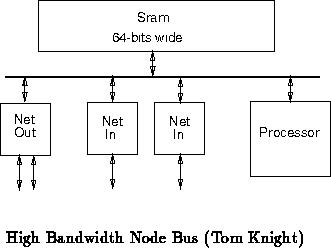
We can gain all of the advantages of the previous (Section )
architecture and achieve greater generallity by doubling the node's bus
bandwidth. Here, we double the bandwidth of the bus by making the memory
twice as wide (Figure
). With memory which can exchange a 64-bit
datum every two network cycles, the node bus has the bandwidth to handle
four devices independently accessing memory at the rate data is being
transfered over the network. This allows the processor, two interfaces
from the network, and one interface to the network to be serviced at full
network bandwidth. As long as each of these components can access memory
at the full network rate, there is no need for separable busses as needed
in the FIFO intensive design (Section
). Also, FIFOs like
those shown in Sections
and
can be implemented in
the flat node memory.
With a single processor, fair emulation is still achievable as described in the previous section. While performing fair emulation, dummy cycles can be used to allow the network to run at full speed as described before. Here, there is no need for the processor to move outgoing data in many cases. It can simply tell the network output interface where in memory to find outgoing data.
Full speed network testing is easier and can be more interesting in this case. Since each agent on the node bus can access memory at full speed, it is easier to keep all network ports busy simultaneously with interesting data while running at the full network rate.
This node architecture will also have reasonably high performance if it is used directly to execute parallel programs. That is, programs can be compiled to directly use the hardware provided by this node rather than emulate the operation of some other hardware. When this is done, this node architecture is capable of using the network at full speed and probably achieving a respectable level of performance.
Features
Bugs
Most of the node considerations are the result of numerous discussions amongst ourselves, Tom Knight, Henry Minsky, and Andy Berlin.