A Fast Static Gate
Thomas D. Simon and Thomas F. Knight, Jr.

We have designed and simulated a new class of static gates with speeds competitive with those of dynamic gates. We call this form of logic SFPL, Source Follower Pullup Logic. implements high fan-in gates in a single fast stage, as well as smaller gates with delays only fractionally larger than inverters. also has small input loading while maintaining reasonable output current. Complex combinational logic functions with small delays can be implemented without any of the disadvantages of dynamic logic.
High fan-in logic gates have applications in PLAs, ROMs, address decoders, or as components in standard cell libraries. Static gate configurations such as fully complementary or gates with pullups are slow and do not scale well with fan-in. High fan-in gates can be implemented from smaller ones by tree cascading, but this incurs several gate delays.
Dynamic logic is faster and scales better with fan-in, but suffers from several drawbacks including tight constraints on the arrival time and polarity of input signals. It is awkward to use at asynchronous interfaces and in timing signal generation.
In addition, large numbers of dynamic logic cells heavily load the clock signals driving the precharge and evaluate devices. These heavily loaded clocks become unwieldy to drive at high frequencies with careful attention to edge placement and on-chip clock skew.
We have designed a fully static single-stage logic form which we call SFPL, Source Follower Pullup Logic. It features delays comparable to the evaluation delays of dynamic logic families. does not require precharging or any clock inputs. gates of five inputs can be made with delays of less than twice an inverter delay. These gates scale up to as many as 30 inputs in a single stage without faster two stage implementations being possible.
We present this new gate design, analyze its performance, and discuss
its noise tolerance and power dissipation. Simulations were run with
HSpice in the Hewlett-Packard drawn channel length
process, the highest performance silicon process supported by the MOSIS
service. No component has yet been fabricated to test this design.
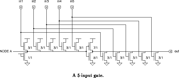
A 5-input gate is shown in figure . It resembles a
pullup configuration, except that (1) the pullup
gate (node A) is controlled by the inputs, and (2) the
pulldown devices can consequently be smaller while maintaining
adequate noise margins and fall time. Node A is controlled by the
inputs through pullup devices used as source followers.
When any input is high the voltage at A is raised, lowering the drive of the and partially turning on the helper pulldown. On the other hand, since the voltage at node A does not reach the positive rail, the is already partially turned on in preparation for a positive edge on the output. The sizing of the devices is chosen so that node A reaches an intermediate voltage (between 2 and 3 volts with a 5 volt supply) when only one input is high.
The advantage over gates is that the slower turn on time of the is traded for less fight against the devices on negative output transitions. This improves both the speed and the low output voltage. In turn, the pulldowns can be smaller than in a configuration. The self-loading on the output node is therefore lower, which compensates for the slower turn on of the P-pullup, especially for large fan-in gates.
When many inputs switch high, node A reaches a higher voltage (no
higher than ). The capacitive coupling from the gates
to the sources of the N-pullups helps bring node A down faster
when the inputs fall. This compensates for the higher voltage change
required to fully turn on the P-pullup.
The source follower configuration of the N-pullups also means
that the loading on the inputs by these devices is relatively smaller
per unit gate width than for devices used as pulldowns,
since there is no Miller effect for the source followers. The total
loading per input is quite small on the gate shown in
figure .
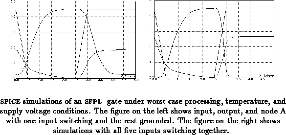
Figure shows SPICE simulations of the five input
gate under worst case processing, temperature, and supply
voltage conditions. The simulations are with only one input switching
on the left and all inputs switching on the right. The inputs are the
square waveforms, the 2 to 3 volt amplitude signals correspond to node
A, with the remaining signal being the output.
As with the configuration, the output of gates are
not rail to rail. The worst case is with only one input high.
gates, however, have lower output low voltages for a given worst case
delay than gates. The device sizes on the gate
shown were chosen so that the output low voltage is 250 mV with
nominal processing and one input high. At the worst process corner,
fast and slow devices, the output low voltage is
500 mV, still 200 mV below . The output levels and noise
margins (discussed later) can be improved at the expense of slower
rising edges on the output, just as with gates.
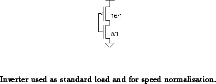
Figure shows the inverter size used for comparison and as
the test load in all simulations. The input or inputs are driven by
voltage sources with 0.5 ns rise/fall times. Propagation delays are
measured from inverter trip point to inverter trip point.
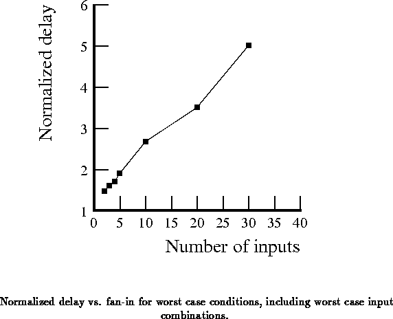
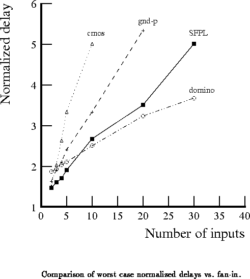
Figure plots worst case delay normalized to the inverter
delay with respect to fan-in, for gates with the same device sizing as
the five input gate. The delay differences grow linearly since
the self-loading grows linearly with fan-in, while the load and worst
case drive remain constant.
By using
-input gates, an
-input gate can be
constructed in two stages. Inverters are required on the outputs of
the gates in the first stage to restore polarity. The delay through
such a
-input gate is twice the delay for the
-input gate plus
some fraction of an inverter delay (a fraction because the loadings are
smaller than for the test inverter). For the device sizings and load
given, the cutoff above which two stage implementations are faster
than single stage ones is about 30 inputs. There are also power
dissipation tradeoffs involved which are discussed later.
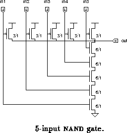
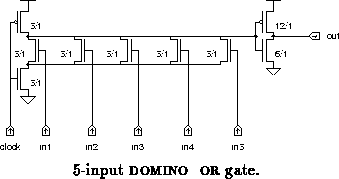
We compare the speed of gates against gates,
basic OR gates [4], and fully complementary
NAND gates. The five input versions of each are shown in
figures through
. The NAND gates used for
comparison have higher input loading than the others. The
has slightly worse output voltage than our gates (in the
worst case
) and about the same static power dissipation.
These results are plotted in figure
. is faster
and scales better than the other static gates. The gates
scale better than SFPL, and are only slower for small numbers of
inputs because of the inverter required for correct
pre-charged output.
The most severe problem in gate design is the static power dissipation, which is comparable to that of gates. Static power is dissipated when the output is low by the at node A and by the which is not fully turned off.
Worst case power dissipation occurs with one input high and the remainder grounded. With more inputs high, the higher current drawn at node A is compensated for by a higher node voltage, which lowers the drive of the P-pullup. For this reason, the static power dissipation does not go up with the number of inputs.
The power dissipated by gates is about 1.2 mW for the device sizings shown and the same process and temperature conditions used with the speed measurements. These same gates dissipate 4.8 mW at the worst power and lowest temperature process corner. This static power dissipation is five to ten times higher than the dynamic power used by or gates with 20 inputs, at 100 MHz, with the given sizings and loads, and at the worst speed conditions.
Because static power dissipation does not increase with fan-in, the
cost in power of using a two stage implementation of a large fan-in
gate is high. A two stage -input gate made of
-input
gates consumes
times the power of the single stage
implementation, with worst case input combinations. Other power-speed
tradeoffs are possible. For example, a
-input gate can be made
from 2
-input gates and a 2-input fully complementary NAND
gate to combine their outputs. This implementation will use twice the
power of the single stage gate, under worst case input logic combinations.
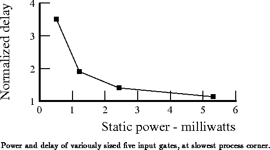
Figure plots delay versus static power for five input gates
of varying device sizings and input loading. As expected, the
delay-power product is not constant. The smaller, slower gates are
more efficient. As devices are scaled up, static power increases
linearly. Speed does not because the self-loading of the gates
increases with the drive. Note that the fastest five input gate size
shown is 10 percent slower than the test inverter. (In fact, the
degenerate single input gate, which acts as an inverter,
and has about the same input loading as the test inverter, is actually
slightly faster than that inverter!)
SFPL, like other static gates, is not susceptible to the noise
and timing problems of dynamic logic. Like grounded- P, however, they
do have poorer noise margins than fully complementary logic.
Figure shows the transfer characteristics of the five
input gate and those of the static fully complementary five input
NAND gate, both with one input varying and with all inputs varying.
These characteristics correspond to process variations with balanced
and device thresholds. The output low noise
margins are about 0.5 volt smaller for our gate. The worst case is
with only one input varying. Figure
shows the
characteristics at the fast and slow process
corner.
These noise margins can be improved at the expense of slower rising edges on the output by changing the relative sizings of some of the devices. For example, the width of the source followers can be increased relative to the size of the on node A. With only one input switching, the voltage at node A will be higher, more fully turning off the P-pullup, and also more slowly turning it back on hard on the opposite transition. With many inputs switching, the voltage at A will remain about the same since the source followers will saturate at the same voltage independent of gate width.
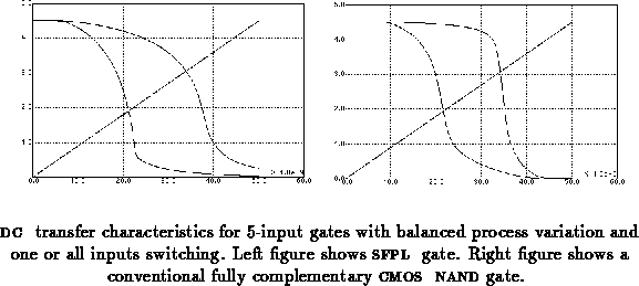
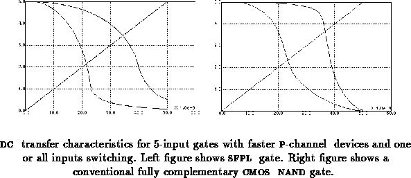
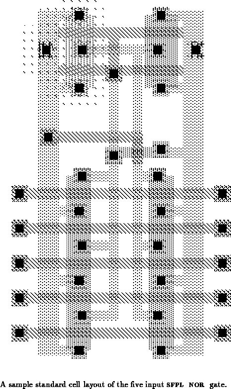
Figure shows a possible layout of the five input gate. The
area is certainly less than twice that of alternative five input gates.
gates can be used to implement random combinational logic such as decoders. The propagation delays are the same for all inputs, as with grounded- P gates but unlike complementary gates or any other logic family with series connected devices. This uniform delay may be useful in timing critical applications such as wave pipelined circuits. They are also very attractive options when both speed and static functionality is needed, such as for generating timing signals.
In addition, it is possible to make single stage and-or gates by
stacking transistors in series, instead of using two stages of gates.
There are tradeoffs of speed, area, and power. The one stage
implementation uses less power and area, but is slower due to extra
loading and the series connected resistances of both pullup and
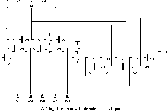
pulldown devices. One special case exception is a high fan-in selector
with decoded select inputs. If constructed as shown in
figure , the single stage implementation is faster than the
two stage one, as well as being smaller and using less power. The
select inputs are connected to the devices closer to the output nodes.
When the select signals have settled, exactly one is guaranteed to be
high and the capacitance of nodes on the other side of most of the
select devices are isolated from the output nodes.
has significant performance advantages over other static logic structures. While does not quite match the speed of dynamic logic, there can be important considerations which make and other static logic attractive, including design complexity, incompatibility of logic with the dominant clocking methodology, and excessive clock loading. In addition, future MOS processes will further scale transistor oxide thickness and channel lengths, requiring simultaneous reductions of circuit voltages. As we scale down both power supply and threshold voltages, the gate continues to function well. In contrast, the subthreshold leakage of MOS transistors becomes a significant problem for all forms of dynamic and precharged logic techniques as we scale to very low threshold voltages. In these highly scaled regimes, either reduction of leakage through low temperature operation, or a fully static methodology, perhaps including gates, will be required.
One disadvantage is the prohibitive power dissipation of SFPL, as with some alternative static logic families, which limits its use to a few thousand gates per die. In any case, gates are one more addition to the set of possible circuits to be considered by careful performance oriented logic designers.
Thanks go to Mark Johnson, Charles Sodini, Mark Santoro, Bob Sproull, Andre DeHon, Nick Carter, Mike Bolotski, and Henry Minsky for their generous suggestions and aid.