DELTA: Prototype for a First-Generation
Dynamically Programmable Gate Array
Jeremy Brown, Derrick Chen, Ian Eslick, Edward Tau
Andre DeHon
Original Issue: November, 1994
Last Updated: Sat Apr 8 21:51:08 EDT 1995

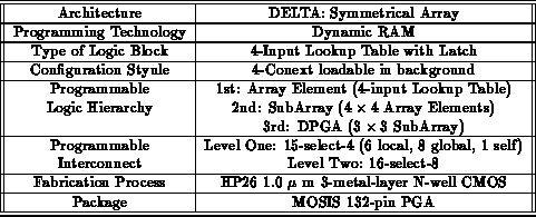
Field Programmable Gate Array (FPGA) has become the industry standard for time- and cost-efficient prototyping medium of digital circuitry. However, relatively few research and applications have gone on to truly exploit the dynamic characteristics of programmability in respect to computational capacity and versatility. Dynamically Programmable Gate Array (DPGA) is a novel concept that aims to time-multiplex different digital configurations of an FPGA in a similar way that a multi-tasking operating system switches contexts to run multiple programs. Conceptually, this is analogous to treating DPGA hardware as virtual-software. Conversely, DPGA's programmable configurations can also be treated as virtual-hardware. From a perspective of system performance, hardware programmability will facilitate a high degree of circuit optimization while maintaining versatility. The motivation of this project is to realize a fully functional prototype of a DPGA in order to explore and demonstrate its potential. The architecture of the prototype is a lookup table-based symmetrical array with two levels of programmable interconnect and four multiple configurations concurrently, as well as background loading of configurations. This prototype will facilitate future research in this direction and also bring forth practical insight of such programmable logic technology.
The primary focus of this prototype DPGA is to explore the architectural issues involved and to demonstrate the utilization potential of flexible, dynamically programmable hardware. Information learned from this first-generation prototype will be used in the design and implementation of second-generation components as well as a DPGA-coupled microprocessor. The Delta prototype features single-cycle context switches, transparent background loading of contexts, and a synchronous DRAM-based memory system. The chip uses a single phase clock with a provision for an external PLL.
Construction of this design is done with the Cadence 4.2.2 CAD tool
package. The prototype chip will be fabricated in the HP26 1.0
m (0.8
m effective minimum gate width) 3-metal-layer
N-well CMOS process and packaged in a 132-pin MOSIS PGA package. The
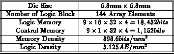
physical die measures
, with approximately a quarter
million active transistors.
Traditional static RAM-based Field Programmable Gate Arrays (FPGA) offer an excellent medium for fast-prototyping of digital ciruit design. The fast in-circuit programmability of FPGAs provides a tremendous time and cost advantage to Mask Programmable Gate Arrays (MPGA), which are asscociated with a high initial overhead of time and cost. Uncommitted resources of FPGAs' circuits permit various configurations of its interconnect, routing, and logic functions. For this reason, FPGAs are especially appropriate for low-volume prototyping of digital circuitry. However, relatively few researchers and applications have gone on to truly exploit this unique and dynamic characteristic of programmability with respect to computational capacity and versatility.
Field-Programmable Gate Arrays (FPGAs) and Single-Instruction Multiple-Data (SIMD) processing arrays share many architectural features. In both architectures, an array of simple, fine-grained logic elements is employed to provide high-speed, customizable, bit-wise computation. A unified computational array model that encompasses both FPGAs and SIMD arrays is first introduced by Boloski, DeHon, and Knight in (tn95). This unified model also exposes promising prospects for hybrid array architectures, the Dynamically Programmable Gate Arrays. DPGA combines the best features from FPGAs and SIMD arrays into a single array architecture.
The in-system reconfigurability of DPGA technology has the versatility to adapt to various system requirements. One way to realize the advantage of DPGA technology is to incorporate it into conventional logic designs. Tight coupling of DPGA to conventional fixed-function computation elements, such as microprocessors, allows application-specific hardware acceleration which is able to adapt as application requirements and usage changes. Such optimizations can be made by compilers which use quasistatic feedback to automatically determine opportunities for hardware acceleration and specialization [DE94].
To extend the virtual-software analogy, a DPGA can be compared to a multi-tasking operating system. In between context switches, an operating system would save the current state of the present task and swap in the state of the next task. Similarly, a DPGA can switch between circuit configuration or a given hardware context on a cycle time basis as required to perform a particular task or process. This multi-configuration/multi-context support is achieved by implementing additional on-chip RAM cells. Each added level of RAM cells will then be able to accomodate an extra circuit configuration. In addition, RAM cells will be integrated to store a given state in order to support the feature of context swap.
The virtual-hardware analogy takes on the circuit level. Utilizing the same circuit real estate of a DPGA to specialize some optimization of a larger module, a DPGA-coupled microprocessor has the luxury of highly optimized sub-systems according to varying needs. A leading example is the role of a small first-level cache that optimizes the overall performance of a much larger but slower memory, and ultimately improves the overall performance of the microprocessor. Furthermore, the fine-grain characteristic and general-purpose nature of the DPGA have the same appeal as that of a general-purpose microprocessor, on a circuit level. Some of the applications of reconfigurable computing elements attached to special-purpose processors or co-processors are appropriate in a variety of situations. The most notable are as follows:
Clearly, DPGAs' high potential for performance optimization in commercial application is beyond the scope of this report. However, future follow-up projects will definitely ensue to explore these issues on a larger scope. These are the motivating factors behind the DPGA project.
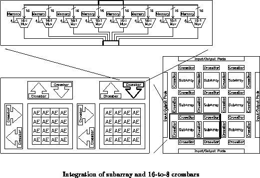
Sixteen (44) array elements are composed into subarrays with
dense programmable local interconnect. At the chip level, nine
(3
3) subarrays are connected by crossbars. Communication at
the edge of the subarrays goes off chip via programmable I/O pins.
Figure
shows the three top-level hierarchies of DPGA's
architecture. Details of each component's implementation will be
discussed in the Modules Section to follow.
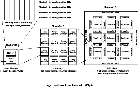
The first level of logic block in the hierarchy is the array element consisting of a simple lookup table which is a universal logic building block. The output of the lookup table can be optionally latched for the purpose of storing state and pipelining. The array element inputs fan in from neighboring array elements as well as from components on other levels of hierarchy. Each array element contains its own memory block to store individual configuration bits, where each set of configuration is a ``context'' programmed to perform a specific logic function. The ability of the memory block to switch contexts in a single clock cycle and the ability to be programmed during run-time are the essence of the ``dynamic programmability'' of the DPGA.
Multiple array elements are replicated horizontally and vertically to
form the subarray, a uniform, and fine-grain logic block. Routing is
crucial to the efficiency and overall utilization of programmable
resources. Within a subarray, array elements can communicate with one
another via intra-subarray interconnect, or level one interconnect.
This level of interconnect runs in both vertical and horizontal
directions across the entire subarray, allowing each array element to
fan in/out from/to the neighbors in the same row and the same column.
A ``local decoder'' contains the logic to control the operation of the
memory block and selects the context of each array element (not shown
in Figure ).
On the top level, subarrays are replicated across the entire chip, interconnected by crossbars, providing flexible routing between subarrays in the level two interconnect. Outputs of each individual array element within a subarray can be selected to fan out to a neighboring subarray in all four directions, providing inter-subarray routing. Programmable configurations of each crossbar are stored in a memory block identical to those in the array element. A high degree of homogeneity is maintained throughout each level of logic block in order to exploit the replicated and uniform nature of the the DPGA. At this level, column and row decodes provide control logic to each local decode. Globally, there are I/O pads that interface outside signals into the subarray grid via crossbars. Programming of all array elements and crossbars configurations make use of the dedicated programming pins which connect to every single memory block.
This section describes in full detail the DELTA implementation. Modules include: array element, memory, crossbar, local decode, subarray, and pads. The section also discusses the pertinent design and implementation decisions as well as other global and floorplan issues.

The DRAM cell uses an aggressive 3-transistor implementation in which
one transistor functions as the read port, one as the write port, and
the third as a storarge device to store a binary bit by means of gate
capacitance. Besides having fewer transistors than a SRAM
implementation, the three-transistor DRAM cell uses solely NMOS
devices and achieves greater speed without the larger and slower
P-devices. Furthermore, the NMOS-only DRAM cell does not have HP26
process's limiting design rule imposed on the N-wells of the
P-devices. Specifically, the process design rules require a minimum
of 4 m N-well to N-diffusion spacing and a minimum of 2.6
m N-well to P-plug spacing. Circumventing P-devices in the
memory block will avoid the above constraints, thereby facilitating
highly compact cell layout.
The design complexities involved in the SRAM implemention resulted in the decision to use DRAM. Proper operation of an SRAM cell relies heavily on applying the appropriate ratio of pull-up and pull-down transistors in its feed-back path. In comparison, the DRAM cell is a pull-down design that does not depend on relative device strength for information storage, which is an electrical advantage. This allows greater freedom in sizing transistors to favor area, performance, and power efficiencies.
The Delta architecture features four contexts, each storing a distinct
configuration that performs a particular logic function. These four
contexts are stored in four cascaded DRAM cells to form a single
memory column (see Figure ). Additional read/write
circuitry in the memory column utilizes a pass gate to charge the read
line to V
, a pass gate to enable connections to the programming
lines or multiplexors, and a refresh inverter to restore the charge.
The refresh inverter also doubles as an output driver in a dual layout
hack.
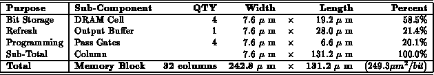
A memory block consists of an array of 32 memory columns, each sharing
the same read/write enable and programming signals. The 32 columns of
4 configuration bits evoke some interesting layout issues. In
particular, the 324 dimensions of the memory block give an
8-to-1 aspect ratio, which is not ideal when trying to construct a
square array element. To balance out the aspect ratio as much as
possible, it is necessary to replicate the individual DRAM cells
vertically. The primary limitation to the minimum width of the memory
block is dictated by the metal one pitch and the contact width of the
HP26 process. After considering the layout topology of the DRAM cell,
layout for a single memory column is minimized down to 7.6
m
wide by 131.1
m tall. With 32 columns stacked along its
width, one entire memory block measured at 242.8
m wide by
131.1
m tall, achieving a desirable aspect ratio of 1.85-to-1.
Read/write operations of the memory are divided into two stages of
system's single-phase clock. The read operation takes place in the
first half of the clock cycle, while the write operation takes place
in the latter half. When the clock goes high, the read line charges
to V. The cell's memory read port is enabled during a read
operation.
If a logical high is stored on the gate capacitance of the pull-down device, the pull-down device will turn on and fight with the pull-up device, attempting to charge the read line. Sizing the pull-down larger than the pull-up assures that the read line will go low. The ratio of pull-up to pull-down is determined through HSPICE simulations of the memory column. Simulated results shows that a pull-down device (1.4/1.0) sized forty percent larger than the minimum pull-up device (1.0/1.0) is sufficient to overcome the fight and pull the read line low within two nanoseconds.
On the latter half of the clock cycle, both the charging device and the read port of the DRAM cell are disabled. The read line, with all gate and parasitic capacitances associated with it, retain the same value from the previous half of the cycle. This value controls the output of the refresh inverter which can selectively drive either the programming lines by enabling the IWE and EWE signals, or drive out by enabling the WE[4] signal. Enabling the IWE and any of WE[0:3] signals will cause the refresh inverter to write a new value into that memory cell.
Pull-up devices are typically implemented using P-devices. However,
in order to maximize the utilization of silicon area, N-device is used
instead for charging the memory column. The tradeoff of doing so is
that the read line is only pulled up to a maximum of one threshold
drop below the power rail, . In this case, the voltage
is approximately
. The
input, though a legal high
according to the inverter, does prevent the P-device of the inverters
from properly turning off. The undesirable consequence is a fight
between the two devices. Two factors in the design of the inverter
assure that the NMOS transistor will prevail in this fight. First,
the N-device turns on with
, versus the
of the P-device.
Second, the NMOS transistor is sized identically to the PMOS. Because
the N-device has greater mobility of electrons than the P-device, the
former's relative strength is about 2
times stronger
than that of the latter, and will prevail to pull the output line low.
In addition to area advantage, the use of NMOS instead of a PMOS
pull-up is better performance-wise due to the reduced voltage swing on
the read line. According to the current-voltage relation , reducing the voltage swing will proportionally
reduce the propagational delay.
The sizes of the transistors used in the memory components are derived from several iterations of design, simulation, and layout. The first iteration started off with minimum sized devices for all transistors. Sizings are adjusted iteratively after running HSPICE simulations to verify the correctness of function. With a working design in simulation, it then becomes possible to construct layouts in order to determine the mask organization. These layouts provided feedback on the feasibility of the design.
HSPICE simulation is the tool of choice for all verification and
performance measurements. Essential functionalities such as read,
write, refresh, and drive are tested with STL vectors in each of the
seven process corners (fast-speed, fast-N-slow-P, slow-N-fast-P,
slow-speed, max-power, min-power, and nominal). The simulation passes
all verfication tests at with a 50% duty cycle clock signal.
Results show the worst case process corner is the slow-speed
simulation.
Another HSPICE simulation has verified the maximum charge-storing
period of the gate capacitance of the DRAM cell. Calculations, using
worst-case HP26 process values and first-order Schottky
approximations, conclude that the charge stored on a 1.0/1.0 minimum
sized N-device is , which takes slightly over
one microsecond to degrade half a volt at room temperature. It is
assumed that the primary source of degradation would be through
subthreshold conduction across the write port, which is approximately
amperes per micron of transistor width. However,
the simulations at the nominal process corner has found considerably
better results. The output waveforms show that the gate capacitance
is able to maintain the charge with less than half a volt degradation
over a period of twenty microseconds. These calculations partially
determine the minimum refresh rate and minimum clock speed of
for which Delta can function correctly.
Analysis of the simulated output waveforms uncovers the low noise
isolation of the gate capacitances within the DRAM cell of read and
write operations. Between the two operations, the read line has a
greater effect of disturbance. Read port passes the charge of the
storage device through the read line. The voltage across the storage
device could either jump from ground to or drop from
to
nominally. Similarly, the write line can affect the charge
stored on the gate capacitance by causing it to either jump from
ground to
or drop from
to
. Little could be
done to remedy these undesirable effects of the read/write
disturbances except by increasing the size of the charge-storing
device. However, this would lead to an even more undesirable tradeoff
of enlarging the layout by a minimum of 10% as required by the HP26 DRC
constraints.
Power dissipation is a primary concern when dealing with dynamic RAM.
This has to be calculated to verify that the IC package is capable of
handling the chip's overall level of heat dissipation. Static power
dissipation in the memory block occurs primarily because the high
input to the refresh inverter is a drop at
, thereby
turning on both the N- and P-devices to create a current flow between
V
and ground.
After a calculated dissipation per memory block, the total of
192 memory blocks in the Delta architecture combine to statically
dissipate a maximum of
. Equally important, dynamic power
dissipation takes place during reads of fighting pull-up and pull-down
devices. At
, dynamic dissipation is calculated at
per context switch per memory block for a total chip consumption of
.
An N-input lookup table can implement any N-input logic gate, at the
cost of storing 2 entries in memory. Given the tradeoffs between
speed, area, and granularity of the functionalities on an integrated
level, a 4-input lookup table, based on research previously conducted,
has been adopted to achieve an overall balance, conforming to most
commercial and academic FPGAs [BFRV92].
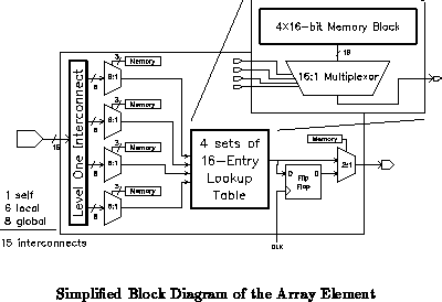
Figure
shows the high-level block diagram of the array
element.
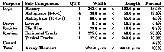
The 4-input lookup table is composed of a 16-to-1 multiplexor where
the 16 lookup entry values are stored in the memory block. The table
output value is selected by four select signals of four 8-to-1
multiplexors. Since each array element can implement 4 distinct logic
gates by storing 4 distinct contexts, the memory required for the
complete 4-context lookup table is 4 16-bit or 32 memory bits,
occupying half of the entire 4
32-bit memory block. The other
half is used by the configuration bits of the multiplexors.
The array element makes use of three different types of multiplexor: one 16-to-1 for the lookup table, four 8-to-1 for the input fan-in selector, and one 2-to-1 for an optional latched output. Two multiplexor implementations are possible: one is a CMOS full-switch implementation using both NMOS and PMOS gates, and the other is a pass-gate implementation using exclusively NMOS gates. The two implementations offer different tradeoffs in power consumption, area, and performance. The design decision, by convention, favors area and performance.
The pass-gate implementation is more area efficient, requiring at most
half of the area as that of the full-switch. However, a high
pass-gate output signal does not reach a full V, degraded from
to
. This degraded voltage raises issues of static power
dissipation when a buffer is used to restore the full V
. One
way to improve the degraded output high is to add a feedback P-device
from the output. This will assist the pull-up to a higher voltage and
mitigate static power dissipation. The negative trade-off of the
feedback is a slower output, resulting from a longer transition period
between valid outputs due to voltage fight between transitive gates.
Calculation shows that static power being dissipated is neglegible.
Therefore, it does not warrant the slower feedback implementation.
The full-switch implementation requires a paired PMOS gate for every NMOS gate to restore voltage by assisting pull-up. However, the cost of implementing PMOS gates is high in terms of layout. In addition to the doubled transistor count, full-switch requires P-devices and N-wells that add tremendous design rule constraints when doing layout. If equal rise and fall times are desired, the P-device sizings must be more than double those of the N-devices. This would effectively triple the gate area required by the pass-gate implementation. Even though full-switch provides a wider channel to reduce resistance in the signal path, the effect on speed by the added capacitance of P-devices is greater than that of the reduction of resistance. The use of full-switch implementation will prove to be profitable only when the load capacitance is large [Seo94].
The array element output drives outwards horizontally and vertically
by means of two 2 size inverter buffers which isolate the
loads directionally. An optional register can latch the lookup output
when programmed active for the purpose of storing state and
pipelining.
The disadvantage of the pass-gate implementation is static power
dissipation. At the end of the cascaded pass-gates, the input to the
inverter buffer will only reach a high of , a value that turns
on both the N- and P-MOS of the inverter. In this situation, current
draws from V
to ground to causing undesirable power consumption
even when the signals are static. The quantitative analysis of power
dissipation calculates that a maximum dissipation occurs at
per
1
size inverter in the worst-case scenario.
The four 8-to-1 multiplexors each have a 2 size (W/L = 2/1)
inverter; the 16-to-1 lookup multiplexor has a 1
size
inverter, and the two output buffers have 2
size each.
Therefore, the total static power consumption for the array element is
With a total of 144 array elements on chip, the upper bound for static
power dissipation due to array element's multiplexors is .
This upper bound is insignificant relative to the other disspation
sources.
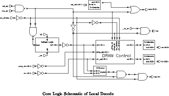
The potential of concurrent memory programming and context-switch warrants conflict resolution schemes. Analysis of DRAM column bus reveals that simultaneous memory reads and context-switch of another contexts will cause a bus-contention conflict. Unfortunately, the only possibility for conflict resolution is to disallow it at the system specification level. All other cases can be handled properly by the logic through a sequence of enable control lines according to the following schemes.
Context switches will always take precedence over reads. Thus, resquesting reads during a context switch will merely produce garbage output. Programming writes may happen at the same time as context switches, since they involve different context write and read lines.
In cycles where neither programming operation nor context switch takes place, the memory cells are refreshed. A counter increments when a refresh has taken place. This will assure that DRAM cells will be properly refreshed despite latencies due to conflicting context switches and programming. During context switches and programming reads, refresh takes place by enabling connection between the feedback inverter and the DRAM write line. Since only one context of memory can be written at one time, cells in the three other contexts may refresh during that cycle.
The first important design decision had a major architectural impact:
pipelining the logic system. Eliminating the latency between pads and
memory from the system critical path will almost double the maximum
operational frequency. Initial simulation shows logic latency from
pad outputs to memory was approximately 6 nanoseconds. This is
unacceptable for the desired 10- cycle time. Adding pipeline
flip flops at the outputs of the decode reduces the delay down to the
time to charge control wires. In this design, control wires are
1500
m minimum-width in metal two and can be driven within
. Slow-speed process corners show this to range from
to
.
The refresh counter consists of two single-phase flip flops with
enable control signals. A transmission gate select-block routes one
of three addresses to the read and write lines seperately. Control
lines for refresh, programming context, and operating context are
routed to read and write signals under the appropriate conditions.
These lines are decoded and then latched by flip flops into pipelined
stages. A 22 comparitor checks for a match of the current
context and the refresh. On a match, the column output charge gets
refreshed with the DRAM cell.
This design is a considerable improvement in performance over the straight logic equations. While other alternatives such as tool-based standard cell synthesis on layouts have not been fully investigated, this design is believed to be nearly optimal. If layout becomes a constraint and other critical paths continue to dominate the cycle time, then alternate implementation strategies will be considered for the subsequent generation of this architecture.
The global lines with the current buffering scheme take a maximum of
to drive the output of pad flip flops to the input of the
local decode logic. With this design, the propagational delay from
valid input to valid output is just under
. The pipeline
flip flops can drive outputs within
under the nominal
process corner, and within
under slow process corners.
The logic has virtually zero static power consumption and has slight
dynamic consumption due to gate capacitance. Power consumption
associated with wire capacitance is less than 5% of gate capacitance
and thus considered negligible. Each local decode consumes
approximately
which leads to a maximum chip
consumption of
due to local decode dissipation.
Special consideration is given to proper spacing between array elements of the subarray in order to accomodate power, clock, ground, and the thirty-two global dedicated programming lines. These vertical lines run exclusively on metal three to feed all the array elements. Additionally, a track is left open for the first stage of clock distribution as dictated by the floorplan.
Crossbars integrate in between subarrays to form the top level floorplan of the chip. This level interfaces the subarray with the the crossbar abutted on each side and an additional local decode to control those four crossbars. This fifth decode fits nicely in the along side with the other four local decodes. At this top hierarchy, it should be evident that the dominant theme in the development of the symmetrical array architecture is to fully exploit the high level of symmetry designed for each component.
The heart of the crossbar is a 16-to-1 multiplexor made of a grid of NMOS pass-gates. The implementation and design decisions are identical to those of the array element multiplexors, though the layouts are individually customized. In each of the multiplexors, four configuration bits decode to select one of the 16 input lines. Four multiplexors with 4 contexts each make perfect use of the 32-column 4-context memory block layout, as does the array element.
Input and output of the crossbar are buffered by sequenced 1
(5P/2N) and 2
(10P/4N) inverters. At the input end, a larger drive
improves the speed at which the NMOS pass-gate grid propagates inputs.
At the output end, the 1
size restores logic levels, whereupon the
2
size drives the actual output line into a subarray. Since each
output line has to drive into 4 array elements (eight 8-to-1
multiplexor input lines), a stronger 2
size driver is warranted for
this larger load.
The decode for each column is implemented as 2-level logic. Sharing NAND terms allows the decode to be constructed in much less area than if each pass-gate is driven from a monolithic 4-input AND gate. Since there is one NOR gate in the decode logic for each NMOS pass-gate in the pass-gate grid, the NOR gate is tightly coupled together with the NMOS pass-gate for an efficient layout snug. As a result, only 8 signal lines have to run from the shared NAND terms into the column instead of 16 from a decode block to its corresponding column of NMOS gates.
Because the number of signal lines needed decreases over the length of the column, wires can become thinner from top to bottom. In another layout snug, a pair of columns is interlocked by rotating one 180 degrees and placing it such that its edges line up zipper-style with the others. The remaining decode logic for each column (inverters and NANDs) is bundled at the corresponding end of the column pair, and laid out such that it smooths out the rough edge created by the abutted columns. Four of these column pairs are then abutted to produce the complete decode and pass-gate grid for the crossbar.
Static power consumption in the worst case under nominal process
parameters is per crossbar, or
over the whole chip.
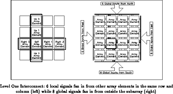
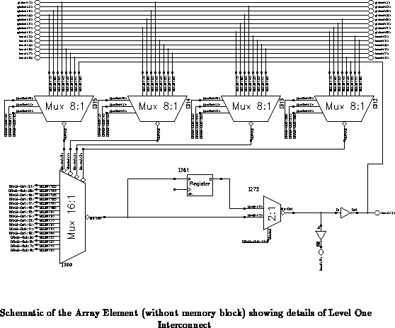
Level one interconnect provides a balanced fan-in of local and global
signals. The incoming local signals originate from the three array
elements of the same row, three more from the same column, and one
self-feedback, for a total of seven intra-subarray signals. The
incoming global signals come from outside the subarray, two from each
of the four directions for a total of eight global signals. The grand
total of Level One signals is fifteen: seven locals, eight globals, and
one self-feedback. The organization of the fan-in signals is shown in
Figure .
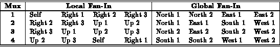
The 4 input-select (8-to-1) multiplexors each use 3 bits per context
for a total of 48 configuration bits. Figure has
details of selectable inputs for routing. The selection scheme allows
the same signal to appear on at least two different multiplexors in
order to augment the total selection combination. Selection of each
input line is arranged in the following fashion:
Interconnect on this level is programmable in the crossbar consisting of eight 16-to-1 multiplexors. Unlike the array elements, subarray can only communicate with its nearest neighbors.
Synchronization and control at the chip level seem deceptively simple but actually involve a great deal of layout and wiring complexity at the floorplan level. For simplicity, all signals in and out of the chip are synchronized to decouple the pad delays from the system critical paths. Control signals are clocked and buffered at the pads and then distributed out across the chip. Programming lines are bi-directional, buffered by a top level pre-pad bi-directional buffer. A reset signal isolates the programmable I/O pins from the external system. This is necessary in order to prevent driving unpredictable values out of the chip during power-up.
Power and ground are provided to the array via pairs of 20-
m-wide wires that form a large grid over the entire chip. The 20-
m-wide wires carry enough current for at most one subarray. The
drop along these wires is less than
(by conservative, but
approximate calculations) under worst case conditions. The subarray
then draws power from these lines into a smaller grained grid across
the array elements. The crossbars operate under a similar scheme.
All other logic draws power from properly sized power rails.
To minimize clock skew, the clock drivers are carefully gridded to
even out current draw. Clock originates from the bottom of the chip,
distributes through the channels between subarrays, and then drives
out via four blocks of large tank buffers onto a clock grid which
spans across the entire chip. Clock lines are m wide for
global wires and
m for local wires (where possible). This
provides a reasonable tradeoff between
noise and capacitive
loading. The clock drives off the chip to form an external phase
locked loop (PLL). The PLL is implemented on chip given the
traditional complexity of such d. To reduce both the pad and the
package delays, a loopback path locks the signals as closely as
possible.
Much of the I/O pad is borrowed from Project Abacus, a VLSI project at
the Artificial Intelligence Lab using a closely related HP26 process.
To reduce pad-ring complexity, Abacus's high capacity DRAM drivers are
used for all I/O signals. The pads were modified in many cases to
include synchronization and output enable logic. Dimension of the
pads are approximately 500 m wide, adding about 18% to the
linear dimensions of the chip.
The MOSIS foundry currently does not carry a CMOS package with more than 132 pins (though GaAs process packages may). While 132 pins is less than desirable due to power/gnd considerations, we have added a great deal of capacitances in the pad ring to compensate for the reduced number of power/gnd pads. We may look for outside packaging sources for the next version of the DPGA.
Testing will be accomplished in two steps. Because the lookup-table-based DPGA is largely composed of random-access memory, testability for most of the DPGA is straight-forward. Verifying input against output bits by applying simple test vectors will suffice for the memory modules and programming lines. After memory verification, testing of the array element multiplexor will complete the testing of the ``logical components.'' Level two interconnect is more difficult to test, since crossbars that are not adjacent to the I/O pads cannot be tested in isolation like memory components. However, crossbars that are adjacent can easily multiplex in simple test vectors into an array element and read back for verfication. These input vectors can be designed by hand and produced with the help of a few simple programs to verify memory contents. Eventually, place-and-route software will be necessary to fully exploit this type of programmable logic.