
Transit Note #114
A First Generation DPGA Implementation
Edward Tau, Derrick Chen, Ian Eslick, Jeremy Brown, and Andre DeHon
Original Issue: January, 1995
Last Updated: Mon Dec 11 14:16:51 EST 1995

Abstract:
Dynamically Programmable Gate Arrays (DPGAs) represent a hybrid
architecture lying between traditional FPGAs and SIMD arrays. Notably,
these arrays can efficiently support computations where the function of the
array elements needs to vary both among array elements during any single
cycle and within any single array element over time. We describe our
minimal, first generation DPGA. This DPGA uses traditional 4-LUTs for the
basic array element, but backs LUT and interconnect programming cells with
a 4-context memory implemented using dynamic RAM. Additionally, this DPGA
supports non-intrusive background loads of non-active contexts and
automatic refresh for the dynamic memory cells. We draw several lessons
from this design experience which may be relevant to future DPGA and FPGA
designs.
Introduction
Traditional Field-Programmable Gate Arrays (FPGAs) have a set of
programmable elements which can be configured to personalize the FPGA to
implement a user-defined function. Reprogrammable FPGAs implement these
programmable elements as memory cells, commonly static RAMs. These
cells are configured during a slow programming phase which typically takes
10's of milliseconds due to limited bandwidth to off-chip memories
[Xil93] [Atm94]. Once configured, the array
personality is static until reloaded. Each array element, consequently,
performs the same function throughout the epoch of operation for the
device. Devices such as the AT6000 from Atmel can support partial reloads
during operation, but the reload still takes a millisecond or more due to
bandwidth limitations, and cells cannot be used during the reload operation.
Dynamically Programmable Gate Arrays (DPGAs) [BDK93]
[DeH94] differ from traditional FPGAs by providing on-chip
memory for multiple array personalities. The configuration memory
resources are replicated to contain several configurations for the fixed
computing and interconnect resources. In effect, the DPGA contains an
on-chip cache of array configurations and exploits high, local on-chip
bandwidth to allow reconfiguration to occur rapidly, on the order of
nanoseconds instead of milliseconds. Loading a new configuration from
off-chip is still limited by low off-chip bandwidth. However, the multiple
contexts on the DPGA allow the array to operate on one context while other
contexts are being reloaded.
In this paper, we describe our minimal DPGA implementation. This design
represents our first generation effort and contains considerable room for
optimization. Nonetheless, the design demonstrates the viability of DPGAs,
underscores the costs and benefits of DPGAs as compared to traditional
FPGAs, and highlights many of the important issues in the design of
programmable arrays.
Our DPGA Features:
- 4 on-chip configuration contexts
- DRAM configuration cells
- non-intrusive background loading
- automatic refresh of dynamic memory elements
- wide bus architecture for high-speed context loading
- two-level routing architecture
We begin by detailing our basic DPGA architecture in
Section  . Section provides
highlights from our implementation including key details on our prototype
DPGA IC. Section summarizes the major lessons from this
effort.
. Section provides
highlights from our implementation including key details on our prototype
DPGA IC. Section summarizes the major lessons from this
effort.
Architecture

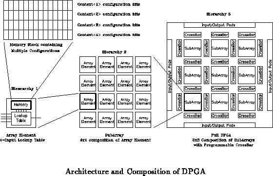
Figure depicts the basic architecture for this DPGA. Each
array element is a conventional 4-input lookup table (4-LUT). Small
collections of array elements, in this case 4 4 arrays, are grouped
together into subarrays. These subarrays are then tiled to compose the
entire array. Crossbars between subarrays serve to route inter-subarray
connections. A single, 2-bit, global context identifier is distributed
throughout the array to select the configuration for use. Additionally,
programming lines are distributed to read and write configuration memories.
4 arrays, are grouped
together into subarrays. These subarrays are then tiled to compose the
entire array. Crossbars between subarrays serve to route inter-subarray
connections. A single, 2-bit, global context identifier is distributed
throughout the array to select the configuration for use. Additionally,
programming lines are distributed to read and write configuration memories.
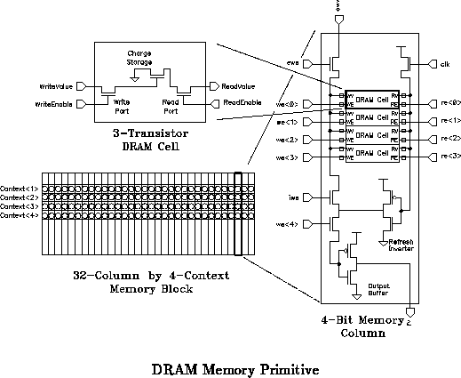
DRAM Memory
The basic memory primitive is a 432 bit
DRAM array which provides four context configurations for both the LUT and
interconnection network (See Figure ). The memory cell is
a standard three transistor DRAM cell. Notably, the context memory cells
are built entirely out of N-well devices, allowing the memory array to be
packed densely, avoiding the large cost for N-well to P-well separation.
The active context data is read onto a row of standard, complementary CMOS
inverters which drive LUT programming and selection logic.
Array Element
The array element is a 4-LUT which includes an
optional flip-flop on its output. Each array element contains a context
memory array. For our prototype, this is the 432 bit memory
described above. 16 bits provide the LUT programming, 12 configure the
four 8-input multiplexors which select each input to the 4-LUT, and one
selects the optional flip-flop. The remaining three memory bits are
presently unused.
Subarrays
The subarray organizes the lowest level of the
interconnect hierarchy. Each array element output is run vertically and
horizontally across the entire span of the subarray. Each array element
can, in turn, select as an input the output of any array element in its
subarray which shares the same row or column. This topology allows a
reasonably high degree of local connectivity.
This leaf topology is limited to moderately small subarrays since it
ultimately does not scale. The row and column widths remains fixed
regardless of array size so the horizontal and vertical interconnect would
eventually saturate the row and column channel capacity if the topology
were scaled up. Additionally, the the delay on the local interconnect
increases with each additional element in a row or column. For small
subarrays, there is adequate channel capacity to route all outputs across a
row and column without increasing array element size, so the topology is
feasible and desirable. Further, the additional delay for the few
elements in the row or column of a small subarray is moderately small
compared to the fixed delays in the array element and routing network. In
general, the subarray size should be carefully chosen with these properties
in mind.
Local Interconnect
In addition to the local outputs which run
across each row and column, a number of non-local lines are also allocated
to each row and column. The non-local lines are driven by the global
interconnect. Each LUT can then pick inputs from among the lines which
cross its array element. In the prototype, each row and column supports
four non-local lines. Each array element could thus pick its inputs from
eight global lines, six row and column neighbor outputs, and its own output.
Each input is configured with an 8:1 selector as noted above.
Local Decode
Row select lines for the context memories are
decoded and buffered locally from the 2-bit context identifier. A single
decoder services each row of array elements in a subarray. One decoder
also services the crossbar memories for four of the adjacent crossbars. In
our prototype, this placed five decoders in each subarray, each servicing
four array element or crossbar memory blocks for a total of 128 memory
columns. Each local decoder also contains circuitry to refresh the DRAM
memory on contexts which are not being actively read or written.
Global Interconnect
Between each subarray a pair of
crossbars route the subarray outputs from one subarray into the non-local
inputs of the adjacent subarray. Note that all array element outputs
are available on all four sides of the subarray. In our prototype, this
means that each crossbar is a 168 crossbar which routes 8 of the 16
outputs to the neighboring subarray's 8 inputs on that side. Each
168 crossbar is backed by a 432 DRAM array to provide the 4
context configurations. Each crossbar output is configured by decoding 4
configuration bits to select among the 16 crossbar input signals.
While the nearest neighbor interconnect is sufficient for the 33
array in the prototype, a larger array should include a richer
interconnection scheme among subarrays. At present, we anticipate that a
mesh with bypass structure with hierarchically distributed interconnect
lines will be appropriate for larger arrays.
Programming
The programming port makes the entire array look
like one large, 32-bit wide, synchronous memory. The programming interface
was designed to support high-bandwidth data transfer from an attached
processor and is suitable for applications where the array is integrated on
the processor die. Any non-active context may be written during operation.
Read back is provided in the prototype primarily for verification.
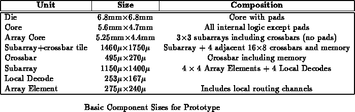
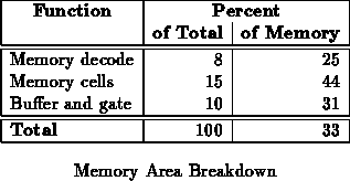
Implementation
The DPGA prototype is targeted for a 1 drawn 0.85 effective
CMOS process with 3 metal layers and silicided polysilicon and diffusion.
The basic composition and area for the prototype is summarized in
Table . From Table , we see
that 40% of the area used on the chip goes into supporting the
programmable configuration memories. Table also
shows that 80% of the area used supports the configurable network.
drawn 0.85 effective
CMOS process with 3 metal layers and silicided polysilicon and diffusion.
The basic composition and area for the prototype is summarized in
Table . From Table , we see
that 40% of the area used on the chip goes into supporting the
programmable configuration memories. Table also
shows that 80% of the area used supports the configurable network.
Layout Inefficiencies
The prototype could be packed more
tightly since it has large blank areas and large areas dedicated to wire
routing. A more careful co-design of the interconnect and subarray
resources would eliminate much or all of the unused space between
functional elements. Most of the dedicated wiring channels are associated
with the local interconnect within a subarray. With careful planning, it
should be possible to route all of these wires over the subarray cells in
metal 2 and 3. As a result, a careful design might be 40-50% smaller than
our first generation prototype.
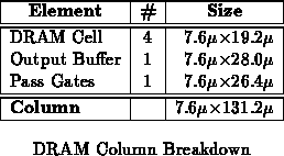
Memory Area
From the start, we suspected that memory density would be a large
determinant of array size. Table demonstrates this
to be true. In order to
reduce the size of the memory, we employed a 3 transistor DRAM cell
design. To keep the aspect ratio on the 432 memory small,
we targeted a very narrow DRAM column. Unfortunately, this emphasis on
aspect ratio did not allow us to realize the most area efficient DRAM
implementation (See Table ).
One key reason for targeting a low aspect ratio was to balance the number
of interconnect channels available in each array element row and column.
However, with 8 interconnect signals currently crossing each side of the
array element, we are far from being limited by saturated interconnect
area. Instead, array element cell size is largely limited by memory area.
Further, we route programming lines vertically into each array element
memory. This creates an asymmetric need for interconnect channel capacity
since the vertical dimension needs to support 32 signals while the
horizontal dimension need only support a dozen memory select and control
lines.
For future array elements we should optimize memory cell area with less
concern about aspect ratio. In fact, the array element can easily be split
in half with 16 bits above the fixed logic in the array element and 16
below. This rearrangement will also allow us to distribute only 16
programming lines to each array element if we load the top and bottom 16
bits separately. This revision does not sacrifice total programming
bandwidth if we load the top or bottom half of a pair of adjacent array
elements simultaneously.
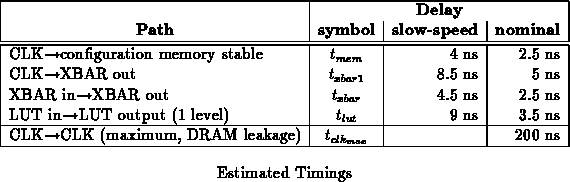
Timing
Table summarizes the key timing estimates for the DPGA
prototype at the slow-speed and nominal process points. As shown, context
switches can occur on a cycle by cycle basis and contribute only a few
nanoseconds to the operational cycle time. Equation relates
minimum achievable cycle time to the number of LUT delays,  , and
crossbar crossings,
, and
crossbar crossings,  in the critical path of a design.

These estimates suggest a heavily pipelined design which placed only one
level of lookup table logic ( ) and one
crossbar traversal (
) and one
crossbar traversal ( ) in each pipeline stage could achieve 60-100MHz
operation allowing for a context switch on every cycle. Our prototype,
however, does not have a suitably aggressive clocking, packaging, or i/o
design to actually sustain such a high clock rate. DRAM refresh
requirements force a minimum operating frequency of 5MHz.
) in each pipeline stage could achieve 60-100MHz
operation allowing for a context switch on every cycle. Our prototype,
however, does not have a suitably aggressive clocking, packaging, or i/o
design to actually sustain such a high clock rate. DRAM refresh
requirements force a minimum operating frequency of 5MHz.
Conclusions
We have presented the full design for a first-generation DPGA prototype.
The prototype demonstrates that efficient, dynamically programmable gate
arrays can be implemented which support a single cycle, array-wide context
switch.
Multiple context programmable gate arrays make the most sense when
moderately small amounts of additional memory area can increase the amount
of logic available for use. While the configurable memory is clearly a
major element of programmable array size in our 4-context prototype, the
memory component does not dominate fixed logic area. With the current
memory cell design, the tradeoff is worth considering, but not necessarily
compelling. If the basic memory cell were much larger relative to the
fixed logic, the memory area would dominate and the multiple context
support would make little sense. Consequently, SRAM-based DPGAs may not be
desirable in the architecture described here.
If the basic memory cell were much smaller relative to the fixed logic, the
logic area would dominate making the cost of multiple contexts marginal and
making it sensible to include even more on-chip contexts. DPGAs with a
more aggressive dynamic memory cell look appealing. Further, DPGAs based
on native DRAM cells or flash memories look very attractive in this
architecture.
See Also...
References
- Atm94
-
Atmel Corporation, 2125 O'Nel Drive, San Jose, CA 95131.
Configurable Logic Design and Application Book, 1994.
- BCE +94
-
Jeremy Brown, Derrick Chen, Ian Eslick, Edward Tau, and Andre DeHon.
A 1 CMOS Dynamically Programmable Gate Array.
Transit Note 112, MIT Artificial Intelligence Laboratory, November
1994.
[tn112 HTML link] [tn112 PS link].
- BDK93
-
Michael Bolotski, Andre DeHon, and Thomas F. Knight Jr.
Unifying FPGAs and SIMD Arrays.
Transit Note 95, MIT Artificial Intelligence Laboratory, September
1993.
[tn95 HTML link] [tn95 PS link].
- DeH94
-
Andre DeHon.
DPGA-Coupled Microprocessors: Commodity ICs for the Early 21st
Century.
In Proceedings of the IEEE Workshop on FPGAs for Custom
Computing Machines, 1994.
[FTP link].
- DeH95
-
Andre DeHon.
DPGA Utilization and Application.
Transit Note 129, MIT Artificial Intelligence Laboratory, October
1995.
Abridged version presented at FPGA '96.
[tn129 HTML link] [tn129 PS link].
- Xil93
-
Xilinx, Inc., 2100 Logic Drive, San Jose, CA 95124.
The Programmable Logic Data Book, 1993.
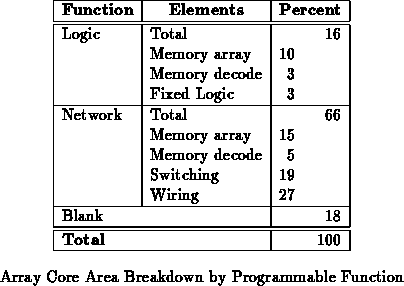
Revisiting Memory Cell Area
From Table , 33% of the 82% non-blank area on the
prototype was supporting context memory. Table
decomposes this  % of active die area.
As noted before, the prototype memory cells were larger than necessary
due to their aspect ratio. Prototype DRAM cells occupied  . In contrast, we expect a tight DRAM cell layout to
occupy
. In contrast, we expect a tight DRAM cell layout to
occupy  in this technology and a tight SRAM cell layout to occupy
 .
.
Assuming commensurate savings in proportion to memory cell area, the
tight DRAM implementation would save about 7% over the current design.
An SRAM implementation would be, at most, 15% larger. In practice, the
SRAM implementation would probably be only 5-10% larger for a 4-context
design since the refresh control circuitry would no longer be needed. Of
course, as one goes to greater numbers of contexts, the relative area
differences for the memory cells will provide a larger contribution to
overall die size.