MBTA: Thoughts on Construction
Andre DeHon
Original Issue: June 1990
Last Updated: Tue Nov 9 12:52:23 EST 1993

This document should detail the construction of MBTA. It is intended to be an evolutionary document. Feel free to add ideas/concerns as they arise.
See [DeH90a] for a discussion of what MBTA is intended to be.
In designing MBTA, we should be keeping a number of goals in mind.
One of the biggest decisions we must make is that of which stock processor to use for the compute and i/o processors. The settled node architecture only has a single node processor [DS90a] so this decision is narrowed to a single processor.
This is a short list of things we were looking for in a processor:
Following is a survey of the various processor available and their various bugs and features.
After much deliberation, we have decided to go with the C series 80960 components. We can start with the 80960CA since it is available now and replace that with the 80960CB when it becomes available. While floating point is essential for the final machine, it is not necessary for early development.
At the moment only 16MHz, 25MHz, 33MHz, and 40MHz versions of the 80960CA are available.
After much deliberation on width, organization, structure, and the like, we decided that the simplest thing to do would be to provide flat, fast, static RAM 64-bits wide. We can always deal with emulated any other memory configurations (including hierarchical, segmented, or tagged memory) on top of this configuration.
The current belief is that we need to support at least 256K words per node (1Megabyte/node). We will provide a 4M word (16M byte) address space on each node so we can expand the memory size if necessary.
The node architecture requires that we cycle the memory twice every four network cycles in full-speed testing mode [DS90a]. With the network running at 100MHz, this requires 20ns memory references. This will translate into needing memory with access time on the order of 15ns.
We want to use the most monolithic parts we can find available. This will
probably be the most economical option on a per bit basis. It will also
save us board space. Right now, it looks like a fast 128k8 SRAM is
the optimal memory component for speed and density.
Note: eventually add information on parts available survey (and pricing) -- this isn't critical, just yet.
For prototyping and building initial MBTA machines it seems optimal to start with some form of Field Programmable Gate Arrays (FPGA's). We should be able to start with these programmable gate arrays and debug logic and functionality. They will certainly not allow us the speed we need to match up to the networks targeted operational speed. With the logic and functionality well understood and debugged, we can then fabricate the logic in gate-array or standard-cell form.
Ideally, we'd like to describe the logic in one CAD tool. From this description, we generate the FPGA's. Once the programmable devices are debugged, we then change to the target technology and ``recompile'' the logic into standard-cell format.
The node architecture is cleanly divided into a few basic units as shown in [DS90a]. The logic units which must be generated are the network interface [DeH90c] and the external bus interface logic [DS90b]. These can each be implemented as its own component. Optimally, we would like to find programmable arrays which allow each of these components to fit in a single programmable package. However, it does not look like any of the current FPGA's have sufficient density. Hopefully, we can find an easy way to divide the logic in each of these components among several FPGAs.
Once the logic is debugged, we can move the designs to standard cell silicon. Ideally, we would like to integrate to as large components as possible. We will probably do the standard cell in the HP26 (1.0 micron process) [HP90]. We can integrate 1V pads into the network interface component(s) allowing the integrated network interface's to connect directly to the final version of RN1/RN2 in the network.
The 4000 series parts is supposed to be more routeable, faster, denser, etc. It also has some level of JTAG boundary scan support [Com90].
8000 gate parts are planned for their second generation components (1232 ``logic modules'' -- where the ACT 2 logic modules may include both logic and a flip-flop in a single module). These parts will support up to 140 useable I/O pins.
Plessey hopes to expand this to 20,000, 40,000, and later 100,000 gates. Plessey has a simple path for moving from these ERA's to Plessey's gate-arrays.
TK's bits on Plessey: The basic cell is either a latch or a 2-input nand gate. Nothing else. There are 2500 of these cells in the part. They estimate 30% utilization after routing for the parts. So the ``10000'' gate part might be more like 800 gates if there are no latches. The wiring is 3 level metal, with some global bus, local bus structure. The local bus hits ten cells. Delay across the chip on the global bus is 5ns. There is also a peripheral bus running around the pads (10 signals) intended for clocks I think. There is a development system on the PC, using Viewlogic capture and simulation, with a programmer. The programmer downloads a two chip module which has the array and a ram to hold configuration info. The module has a large capacitor to hold config information for 24 hours unpowered. It has the identical pinout to the real part, and can be plugged in in place of the part in a system environment. They seemed receptive to the idea of letting us get in and muck with the intermediate formats and the detailed routing. The development system cost $10K and comes with 2 modules. The modules cost $500. The parts are $200 in 1-25, and $70 in 250-500.
We settled on using Actel FPGA's and are now set to program the ACT1 series components. In theory they are in the processor shipping us a programming head to allow programming to the ACT-1280, the large ACT2 component.
The T-Station host interface is described in [DeH90d]. We have settled on using GPIB [Com78] as the initial transport layer for implementing the T-Station interface. This decision was made as the result of a number of goals:
It may be desirable to eventually provide other T-Station implementations. As mentioned in [DeH90b] an ethernet T-Station might be interesting and would free T-Station from needing a dedicated host machine.
How do we integrate conventional packaging into our stacks?
Tony Salas is looking at this problem in his 3-D DRAM project. Hopefully, the insight and experience gained in packaging conventional DRAM parts in a three-dimensional structure will be applicable to our more general problems.
Options for consideration include:
See [DeH91].
This is largely outdated -- see [DeH91].
Current projections suggest that the 64 processor ( routing
components) routing boards will be about
square.
At the ends of the network, this leaves us with about a
square area centered around each routing component where
four nodes need to connect. If we place half the nodes above the network
and half below it, then two nodes need to connect to this
square area on each side of the network. For this
arrangement one way to package the nodes would be in small vertical stacks
which are roughly
square and 3 or 4 layers tall.
However, a rough cut at the design for a multiple layer
square node such as this exposed a few problems with such a strategy. The
amount of vertical interconnect required for a node spread over
multiple layers is quite large. Also, breaking up the space into these
small amounts severely limits our ability to effectively use the available
space.
Alternately, we are current considering square nodes.
Assuming we can build a node this small, the node spans 4 (
)
routers. This way 16 node boards are needed for each cluster of 4 endpoint
routers. If we split the nodes on either side of the network, this means 8
nodes reside on the each side of the network. This strategy allows us to
exploit planar interconnect within a node where things are heavily
interconnected. It requires only minimal vertical interconnect since each
node only requires the 40 signal pins necessary to be connected to the
network.
The exact details of what we will need to package into each node will
depend on the level of integration we can get away with.
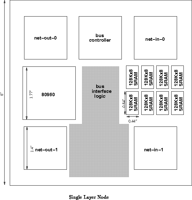
Figure shows a possible single layer node. Here, we use
the through vias provided by the Transit-DSPGA372 package to effect
vertical interconnect. Together, four such packages provide just enough
through bandwidth to satisfy the requirements of eight nodes. This allows
us to use basically the same packaging scheme for the nodes as we do for
the network. To effectively do this, we do have to get all of our random
logic packaged in thin (less than 110 mil thick) packages. A quick check
looks like this is doable using leadless or gull wing surface mount
components. This configuration is tight and may be tough to route.
If we can package the 80960 in a Transit-DSPGA372 package and
integrate four network interfaces into a single VLSI component which is
also packaged in a Transit-DSPGA372 package, we can further cut down the
component area requirement and make a single layer
square node more feasible.
In either case, we will need two different flavors of node boards. Since the board is square, we can use the four possible rotations of the board to tap off four different sets of network ports for four nodes. However, we need to tap off eight different sets for each side of the stack. We can make two slightly different boards which tap off of the node at different places on each rotation.