MBTA: Node Architecture
Andre DeHon
Thomas Simon
Original Issue: July 1990
Last Updated: Wed Nov 10 23:36:18 EST 1993

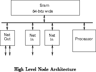
A rough diagram of the MBTA node architecture is shown in
Figure .
The node
architecture is simple with a single processor and memory. The fast,
64-bit wide memory is intended to cycle at four times the rate at which
data arrives from the network. The node is, thus, capable of utilizing
full network bandwidth through two network inputs and a network output
while still allowing the processors regular access to memory.
This node architecture allows fair emulation since there is a single stream of execution. The processor can simply executes a time slice of each emulated node device during each emulation cycle.
In fast network test mode, the processor can feed raw write operation over the network at full network speed and record the appropriate statistical information. The write operations are handled directly by the net-in units, leaving the destination node's processor free to check received data and setup outgoing data. Once a transfer is setup net-out operates autonomously from the processor.
When emulating nodes, it would be unfair to run the network at full speed.
The network should only be running at some small fraction of its real speed
to be fairly matched to the simulation. However, it is important in
testing reliability and cooling to be able to run the network at full speed
for long periods of time. To allow these test to coincide with emulation
experiments, net-out and net-in can both be configured to send
``dummy'' data to consume the unused network bandwidth. Rather than
running the network slow, net-out and net-in are designed to
service the network at full speed. However, they do not send simulated
data at full speed. They will send the node generated network data only
intermittently. Between these times, they will send filler data to each
other. Both endpoints agree to only treat every -th byte as network
data (where
is a parameter set at boot time). Between the valid data,
the sending node sends some sequence of random data which the receiving
node can anticipate and verify ( e.g. the sending node could simply
send the contents of a byte wide counter running at network speed). This
allows the nodes to see network bandwidth which is properly matched to the
emulated node speed. At the same time, the network can be run continuously
at full speed with semi-interesting, changing information running through
it. All of the interesting packaging, cooling, and reliability issues can
thus be tested simultaneous with simulations.
The node can also be configured to execute programs directly in fast mode. That is, the number of dummy cycles can be set to zero and code can be run on the raw node hardware, rather than an emulation. The bandwidth provided by the fast, wide memory allows all network interfaces to access memory fast enough to satisfy the bandwidth to and from the network.
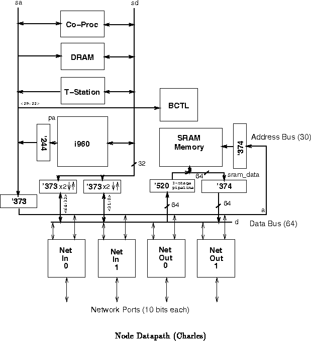
Figure shows the primary datapaths for an MBTA node as
composed of the components described here and in (tn20), [DS90b],
and (tn75).
Twenty-four address bits are allocated for referencing memory within a node. This gives each node an address space for 4 megawords (16 megabytes). The current plan is to provide each node with only 256 kilowords of memory; this scheme leaves room for larger memory in case 256K words proves constraining.
Since the 80960Cx deals with 32-bit byte addresses (30 bit word addresses), one way of referencing global shared memory is to use the top 8 bits of a 32-bit shared memory address as a node number. This gives the ability to address 256 nodes while addressing the full 16 megabytes of address space on each node. Software is, of course, free to perform any mapping appropriate to derive a node number and a 24-bit node memory address.
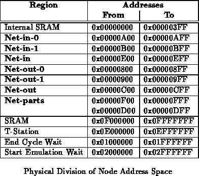
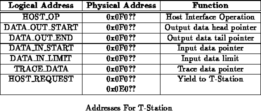
Table shows the physical division of a node's
address space. The Net-out address is used generically to reference
the single logical network output interface device. The specific addresses
for net-out-0 and net-out-1 are provided for diagnostic and
configuration use when it is desirable to reference a particular network
output unit. Net-in is used to generically reference the network
inputs and Net-parts is used to generically reference all network
components. Needless to say, these addresses may be used for simultaneous
writes, but should not be used for read operations.
These network addresses are mapped into the low memory
region just above the internal SRAM so that they can be addresses with
short addresses. These addresses are all 12 bits long and fit in the
80960's short constant field for read operation.
N.B. This is a recommendation for how to manage host-io. Software is certainly free to do something else as long as it is consistent.
The T-Station host interface requires seven memory words located in the
node's SRAM for communication (see Table ) (tn20)).
The HOST_REQUEST memory address is also used to allow the
processor to yield to T-Station (see Section
below).
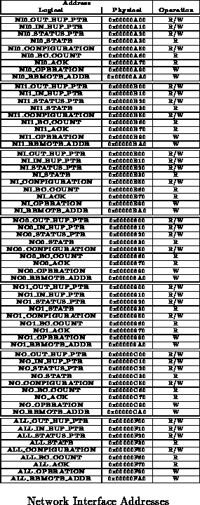
Net-out and Net-in each require several addresses for
communications. These are all mapped into the memory mapped I/O portion of
memory. Table summarizes the addresses used by these
components. The network Interfaces are detailed in (tn75).
After the processor has emulated everything it is intended to emulate for a
given emulation cycle, it must wait for the end of the cycle to occur
before continuing. This is necessary in order to keep emulated cycles in
relative synch between all the processors in the machine. To effect this
wait, the processor issues a read to EC_WAIT. The
nodes bus controller recognizes a read to this address and does not give
the processor the signal until the end of the emulation
cycle has occurred. The bus controller is informed about the end of cycle
by the assertion of EC by the master net-in.
After the nodes go through the boot and initilization sequence, each node
must wait for emulation to begin before it can start running its emulation.
This wait is effected similarly to the end of cycle wait. The processor
will issue a read to EM_WAIT. The nodes bus
controller recognizes a read to this address and does not give the
processor the signal until
is asserted
inidicating that emulation should begin.
N.B. In general, this gives each node to wait on the assertion of a single global signal. This facility could be used during run-time as a form of barrier-synchronization.
As described in Section dummy cycles are inserted between
real network cycles to allow the network to run at full operational speed
while the processor uses many processor cycles to emulate a node cycle.
The number of dummy cycles between each pair of real network cycles is
configurable. This will be configured once during the boot sequence so
that all nodes agree on the ratio of dummy cycles to real cycles and when
the emulation cycle ends.
As part of keeping the nodes in synch, real network cycles should be in synch. That is, connection opens which would have occurred on the same network cycle in the emulated machine should occur on the same network cycle. This guarantees to properly test network congestion and to properly test opening connection at full speed.
The dummy/filler data should have the following properties:
One consideration is to send the value of a counter which counts from one's node number up to one's node number plus the number of dummy cycles. This would guarantee dynamic, testable data which differs from node to node. Another possibility is to xor in one's node number to a counter which runs from zero to the number of dummy cycles. While the later is probably computationally cheaper, it may not provide sufficiently different data between nodes in many cases.
This section describes the current thought on the value of dummy data.
The dummy data can be the last data value sent (or received) xored with a counter which runs up to the specified number of dummy cycles. e.g. the data sent would look as follows:
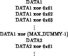
This strategy has the following nice properties:
The processor will be a C-series 80960. We are using the 80960CA [Int89c] [Int89b] [Int89a] for initial prototyping and development. Later MBTA machines will use the 80960CF. The 80960CA and 80960CF are pin compatible. The only difference between the CA and CF processors is the instruction cache-size and the existence of a data-cache only on the CF.
A 25MHz (40ns) processor seems best matched to the node architecture. This makes the processor clock an even multiple of the network clock (10ns) and the targeted memory cycle time (20ns). It is not immediately apparent how we would properly utilize a faster processor.
The processor will be run in the Two-X clock mode. Pipelined addressing will be used to obtain the most bandwidth from the memory system.
The high speed memory will need to provide a memory cycle to each of
four devices (2 net-ins, 1 net-out, and the processor) every
80ns to match bandwidth with the network which can transfer 8-bits of data
every 10ns through each network port. Each device, thus, has roughly a
20ns memory cycle. This means we will need 15ns SRAM.
In general, each device will get a single turn at memory every 80ns cycle. Each network interface indicates to the bus controller whether or not it will be using the bus during its designated 20ns memory cycle. Each network interface knows its cycle and uses it without any explicit acknowledgment from the bus controller. If a network interface does not indicate a desire to use its designated cycle, this cycle may be used by the processor to reference memory.
The processor can only deal with 32-bit data transfers. Muxes are provided so the processor can obtain access to either the low or high memory word as necessary. The node bus controller deals with enabling tristate buffers appropriately.
To accommodate the need for fast memory cycle times (20 ns), pipeline
registers are placed immediately before and after the memory components, as
shown in Figure . The memory components used will not have
built-in registered inputs or outputs.
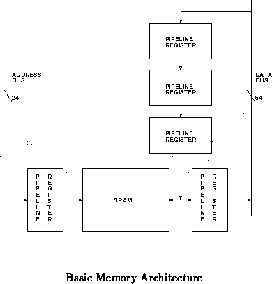
The pipeline registers separate various sources of latency into
separate 20 ns cycles. Thus each of the following components of access
latency occur during separate pipeline stages: address settling on the
address bus, the memory component access latency, and data settling on the
data bus (for reads). There are three stages of pipeline registers for
write data so that the data will become available at the I/O ports of the
memory components during a given devices memory access time ( i.e.
at the same time as the address from the associated client device). Read
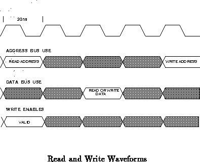
and write waveforms are shown in Figure .
Read data is available on the data bus during the client's allotted slot on that bus. The address of the read operation must be asserted during the same client's address bus slot which is always two 20 ns cycles before the client's data bus slot. For writes, the write enable signals are asserted on the cycle before the data; the data is placed on the shared data bus during the subsequent cycle; finally the corresponding address is placed on the shared address bus two cycles later than the data.
This phase difference between address and data cycles for each client
was chosen to minimize the latency of read operations. This latency is
most critical to the processor. Figure shows the
interleaving of the memory requests of all four clients.
Needless to say, each client must only drive data onto a shared bus (data, address or enable controls) during its own cycle. A client's drivers should be in a high impedance state during cycles not alloted for its use.
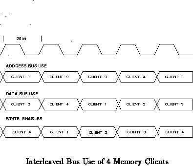
To allow the processor to borrow extra unused memory cycles, each network interface part must provide a bus wanted signal ( WB). This signal should be asserted during the cycle preceding the client's allotted address slot. It should be asserted if the client intends to use either its following address cycle or its next data cycle (three cycles following the busy signal). If the WB signal is not asserted the bus controler may use that client's next address and data cycles to perform a read operation requested by the processor.
If we had some way of knowing when two sequential sets of cycles were left unused by the same client, we could allow processor writes to be serviced during borrowed memory cycles. However, this information may be hard to generate and keep up with so we will not supported borrowed write cycles. Only reads will be serviced during borrowed cycles.
The T-station host interface will always perform memory operations strictly during the processors allotted bus cycles.
The processor may also perform reads and writes directly from and to any of the interface parts. If an interface part is addressed by a processor read, it must drive the required data onto the data bus during the processor's allotted data cycle. To facilitate writes, each interface part must cache the contents of the data bus during the processor's data cycle on every such cycle. The address, along with a chip select indicating the address is intended for some network component, will be provided 2 cycles later, at which time the network interfaces can determined who is being addressed by the write operation.
Note, that all network interface control addresses are quad-word aligned. This allows the network interface to only listen to the low word of the data bus for processor transactions.
The node bus control ties the processor, host interface, memory, net-out, and both net-ins together. The bus controller is described in detail in (tn30).
The bus controller handles the following tasks:
The network interfaces deal with moving data to and from the network. Two net-in units service two network ports into the node from the network. Two net-out units interface to two ports into the network. Only one of the two net-outs will be used at a given point in time. Two are provided for fault-tolerance; when each network output transaction is initiated, they arbitrate with each other to decide which unit handles the transaction. The function and usage of the network interfaces is described in (tn75).
Note that an MBTA node has no hardware control for atomicity. Any hardware atomicity control we might have added would interfere with the emulation where many cycles of processor execution are being expended on emulating one cycle of each of several pieces of emulated hardware. It is not appropriate to lock out the emulation from execution. Software interlocking should be used to emulate various atomic/locking schemes on the node. This leaves all of the details of assuring emulated-atomicity to software.