MBTA: Node Bus Controller
Andre DeHon
Thomas Simon
Original Issue: August 1990
Last Updated: Mon Nov 8 13:42:47 EST 1993

The node bus control ties the processor, host interface, memory, net-out, and both net-ins together.
The bus controller handles the following tasks:
The node bus controller will deal with directing processor memory
references to the correct units. That is, it will generate the appropriate
chip select and control logic for the various memory mapped units.
Table shows the relevant mappings.
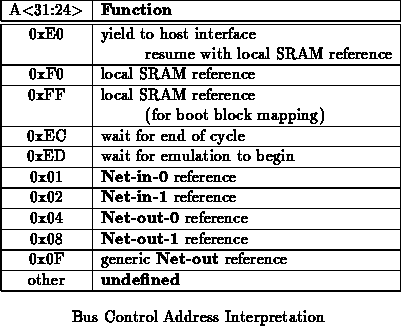
The node bus controller will need to map the boot block into the a region
of real memory. As mentioned in (tn25), Intel insists the boot block
reside in an otherwise unusable section of memory [Int89c].
To satisfy this requirement, the bus controller locates the node's SRAM at
two locations as shown in Table . Host interface yields
complete by obtaining a return value from the node's SRAM memory. Thus,
the host interface yield addresses are simply SRAM addresses with a special
function preceding the actual memory operation.
The node bus controller must deal with three special function addresses. These are the HOST_REQUEST, used to yield control of the node to the host interface, EC_WAIT, used to hold until the end of an emulation cycle, and EM_WAIT, used to stall the processor until emulation begins.
The node bus controller intercepts reads to the HOST_REQUEST
address. It keeps deasserted and asserts HREQ to
indicate to the T-Station interface that the processor has yielded control
of the node to the processor. At this point, the controller also asserts
HOST_BUS to inform net-in that the host interface has
control of the node bus. The node bus controller forwards the host
interface control signals straight to memory allowing the host full access
to the node's SRAM memory. Host access to the node's memory is not
performed in pipelined addressing mode. When the host is finished, the
host interface will assert
. The node bus controller then
completes the read operation to the SRAM address associated with
HOST_REQUEST. The node bus asserts
to the processor so
that it can continue and deasserts HOST_BUS. (tn20) explains
more about yielding to the T-Station host interface.
The node bus controller intercepts reads to EC_WAIT and holds
the processor until the end of the emulation cycle. The controller simply
keeps deasserted until the processor cycle following the
deassertion of EC by the master net-in (see (tn31) for
more details).
Currently, the data returned from the read to EC_WAIT is undefined. Is there anything interesting (and easy) to provide as the completion of this read, or shall we not bother?
After the nodes go through the boot and initialization sequence, each node
must wait for emulation to begin before it can start running its emulation.
This wait is effected similarly to the end of cycle wait. The processor
will issue a read to EM_WAIT. The nodes bus controller recognizes
a read to this address and does not give the processor the
signal until
is asserted indicating that emulation should
begin.
Currently, the data returned from the read to EM_WAIT is undefined. Is there anything interesting (and easy) to provide as the completion of this read, or shall we not bother?
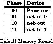
The node bus controller is also responsible for coordinating memory
access among all devices on the bus. During each memory round (8 network
clock cycles), each of the four logical bus devices ( net-in-0,
net-in-1, net-out, and the node processor), may access the memory
once. Each memory access will complete in two network clock cycles.
Normally, each of the devices will access the memory once during its
designated portion of the memory round. However, if a network interface
does not need to use its memory access cycle during the round, the processor
can get a second memory access during the memory round. The basic memory
round is shown in Figure .
The network interfaces share a want bus ( WB) signal. When a
network interface needs the bus on a given round, it asserts WB
and the word enables (<1:0>). See (tn31) for
details on timing. If the network interface does want the bus, then
the bus controller will not allow the processor to access the memory
during the designated memory access. The bus controller will assert
the appropriate SRAM enables based on the network interface's write
enable specification. Note that each network interface will always
get a memory cycle when it wants it. Only one of the net-out
units should request a bus cycle during any memory round since the two
net-out units logically act as one network output.
The processor always gets an opportunity to reference memory during it's designated memory access cycle when it has a memory reference pending. If net-out does not assert WB sufficiently prior to its designated memory cycle and the processor has a pending memory reference, the bus controller allows the memory cycle to service the processor's pending memory reference.
During the processor's designated memory cycle, it can reference any of the
network interfaces. The bus controller uses W/ and
to inform a network interface of a reference from the
processor. These signals are separate from the network interface's write
enable selections so the network interface can set up its memory reference
regardless of references from the processor.
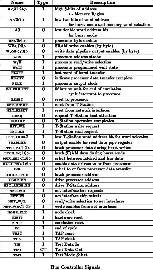
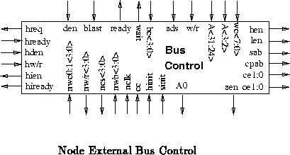
Table summarizes the signals associated with the node
bus controller. Table
is more authoritative
with respect to signal polarity than the figures. Table
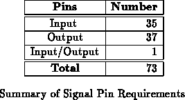
summarizes the pin requirements for the node bus control unit.