MBTA: Clocking Strategy
Andre DeHon
Original Issue: January 1991
Last Updated: Mon Nov 8 16:10:57 EST 1993

MBTA will be composed of 48 RN1 components and 64 nodes. These components will be distributed over printed circuit boards approximately 16 inches square. Communication among components in the network portion of the machine is not limited to local communications so some connections may easily be 2 to 2.5 feet long. The RN1 components will be transferring data with each other and with the nodes at 100MHz while most of the logic in each node runs at 50MHz. RN1 will require a 1V clock while the conventional components on the node will require 5V clocks.
For a more detailed description of MBTA packaging, see (tn33), (tn17) [DeH90c]. The salient points are reviewed briefly here.
The entire MBTA machine will be packaged in a three-dimensional stack. The
network makes up the central layers of the stack. It is composed of 3
layers each with 16 routers; each layers is arranged in a
configuration. The size of these routing layers will dictate the overall
packaging size. Current effort at routing the horizontal routing boards
required to interconnect routers indicates these boards will be slightly
under 16 inches on each side. Half of the nodes will be packaged above the
network and half below. Each node will occupy one fourth of a layer
in the stack ( i.e. each node will fit in the space of 4 routing
components allowing 4 nodes to be packaged in a single stack layer). In
this manner, 8 layers of nodes above and below the network will comprise
all 64 nodes. Each layer in the stack, including components and printed
circuit boards, will be about 250 mils tall. The entire stack will thus be
.
DSPGA372 packages and BB372 connectors will be used for vertical
interconnect.
The following summarizes the basic strategy to avoid clock skew problems:
RN1 is constructed using Alex Ishii's 1V pads. As such, the component needs to see a clock which swings zero to one-volt. We can use biased ECL clock drives and buffers to provide this clock to the router. ECL drivers are better suited for providing high speed clocking and driving transmission lines in this manner.
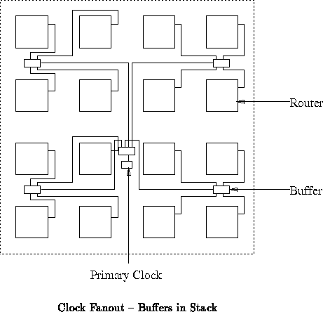
The central clock is buffered and fanned out to the four quadrants of the
central printed circuit board. There, the signals are buffered again and
each of the component columns is driven with a single buffered output. The
columns interconnect the components needing clock inputs vertically. Here
the distance is short (approximately 2.5 inches in each direction) so signal
skew on vertical signal propagation is not a major concern. This clock
distribution is run open loop assuming the ECL buffers are all tightly
matched. The fan-out
traces should be matched so that they are all roughly equal length.
Figure
shows how this fan-out will be arranged if we can
manage to place the clock and buffers inside the stack structure.
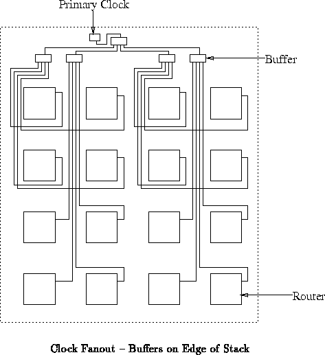
Figure
shows the alternative if we must package these parts
outside of the main stack structure.
N.B. Since we probably are not routing on the surface planes of each horizontal board, it might be reasonable to surface mount the clock and buffer components on the top of one of the middle routing boards. We can fanout the clock on the surface layer and avoid congestion and crosstalk between the clock lines and the routing traces.
Each router and network interface will be located in one of the 16 columns of components. Each thus sees a 1V clock signal with only minimal skew due to vertical distribution.
The important observations we make here are:
Thus, as long as the network interface is implemented such that it listens to both the node and network clock and the frequency of the clocks is in the proper relation, there can be a bounded amount of phase delay between the node and network clock. The network interface components generate a 5V output clock for the node at half of the frequency of the network clock it receives. The operation of generating this clock and driving it onto the node will skew the output clock somewhat from the input network clock. This output node clock can then be buffered, perhaps adding further skew, and distributed to all agents on the node requiring the node clock include the network interface component. In this manner all communications on the node occurs with respect to this buffered node clock. The network interface uses this clock to control the portion of the component which communicates directly with the node so that its communication is properly synchronized.
Based on the current scheme for bridging the portions of the network
interface which run on these two clocks, Equation , bounds the
amount of skew which can occur on the node clock. These bounds are derived
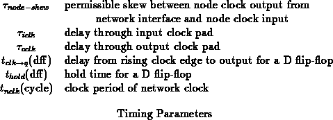
with the implementation description in (tn36). Table
summarizes the parameters used in Equation
.