Network Interface
Implementation Notes
Andre DeHon
Original Issue: January 1991
Last Updated: Mon Nov 8 14:52:15 EST 1993

This document is a serious of notes on the implementation of the network interface component.
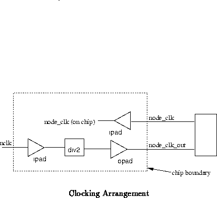
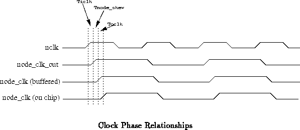
Figure shows the phase delays between the various clock
signals shown in Figure
. This diagram underscores the
point that there will be a non-trivial phase difference between NCLK
and NODE_CLK. Table
shows names the timing parameters
used throughout this description.
Since the network interface runs on two distinct clocks, care must be taken
in communicating between portions of the design clocked on different
clocks. Figure shows the configuration for synchronizing
signals between the two clocks. All network interface flip-flops, except
for those communicating directly with the node, are clocked with
NCLK. Those communicating with the node are clocked with
NODE_CLK. We synchronize control signals from the FSMs to flip-flops
running from the NODE_CLK by using a single D flip-flop clocked by
NCLK. This strategy has the effect of holding all control singals
past the end of an NCLK cycle so they are valid at the end of the
corresponding NODE_CLK cycle.
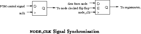
This strategy puts a few constraints on the skew between NCLK and
NODE_CLK. First, the control signals clocked into the
synchronizing D flip-flop must be valid on the output of the D flip-flop
prior to the rising edge of NODE_CLK. This requires that the
phase difference be at least as large as the time for data to settle on the
flip-flop outputs following a rising clock edge ().
Additionally, the rising edge of NODE_CLK must occur sufficiently before the next rising edge of NCLK to meet the hold times required for the control signal.
With the synchronization strategy just described, we must still follow a discipline in providing data and control to these flip-flops.
Three FSMs control the flow of data through the network interface component. The proc-io FSM handles read and write operations directly from the node processor to the network interface. Node-out handles the task of writing out network data to the node memory in accordance with the node's bus discipline. The central FSM coordinates all activity between the node and network.
The cannonical source for these state machines currently resides in:
/home/ar/transit/mbta/ni/ucb/. All state machines are qualified with the extension .scm.
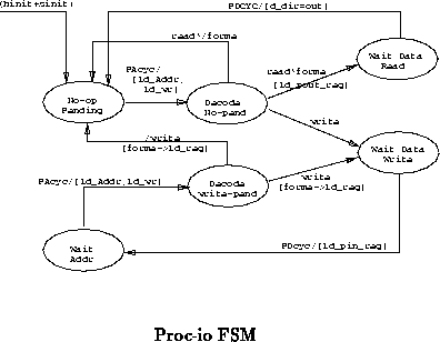
This finite state machine recognizes bus transactions requiring the node's attention. As such it services all read and write operations performed to the network interface.
Figure shows the basic behaviour of the proc-io FSM.
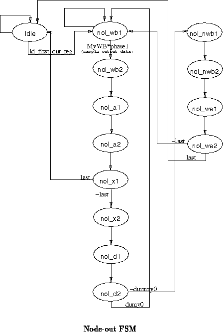
The node-out FSM deals with staging data and coordinating with the node bus controller to write data out to node memory.
Figure shows the basic flow of control in the node-out
FSM. To make the diagram readable, signal assersions have been omitted
leaving only the basic state machine flow. Loopback arrows with no
qualification are taken when the condition on the exit arrows are not
satisfied.
The primary difficulties in this state machine are dealing with the arbitrary phase skew (relative to component's bus cycles) of data arriving on part. This skew arises because of skew in the sender due to which network part is sending (and it could be any of the 4) and how many stages of network exist; this is componded by the fact that there can an arbitrary number of dummy cycles. This means that the data can arrive on the part at virtually any phase relative to the components cycles on the data bus. It could happen that the component gets a full chunk of data to write out just in time to stage it and write the data out on its bus cycle. It could also happen that the data could arrive just one network cycle (10ns cycle) too late requiring that the data be held an entire emulation cycle before being offloaded to memory.
The consequence of this is that some effeciency in hardware and latency
through the part is sacrificed to allow this generallity. Given a number
of dummy cycles and phase of arriving data, I'm sure it is possible to
derive an optimal sequence of data manipulations that minimize latency --
however I don't believe it is possible to derive one that works with the
generallity necessary. The data must be double buffered before being fed
to the final output buffer. This ineffeciency arises because the final
output buffer is clocked on NODE_CLOCK and hence must be valid
across two cycles; however, since the phase can be shifted by any amount,
it is not possible to guarantee that the data will be stable for any two
clock cycles. Instead, we must be able to transfer incomming data to
staged data in one cycle. The staged data can then take the two clocks
necessary to transfer to the final output register. Also, it would be
possible in some cases to note that data will be available a set number of
clock cycles in the future and start arbitrarting for bus access before the
data is actually ready to be transfered to the staging registers. However,
since there can be an arbitrary number of dummy cycles it is not possible
to make this prediction with sufficient generallity in a simple manner.
Thus, the current solution is inefficient in these manners. Perhaps, it
can be optimized some after everything else is working.
Note in Figure that there is a branch of the FSM taken
when DUMMY0 is not asserted. DUMMY0 flags the particular case
in which the number of dummy cycles is set to zero. In this case, write
operations are overlapped with enable and want bus signals for the next
write asserted with the address for the last write. In all other cases
( i.e. the number of dummy cycles is greater than zero), writes
start and complete in the two node cycles following end of cycle and are
not overlapped. See the end of cycle timing diagrams in (tn31).
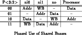
(tn31) describes when each network interface part and the processor
reference the shared data, address, and control busses. In setting this up
in the network interfaces, I found a table as shown in Table
useful.
SINIT should not reset the phase of the network parts with respect to the phase set by HINIT. Resetting the phase could leave the 80960 out of phase after SINIT
Things reset by HINIT (only):
Things reset by SINIT (only):
Things reset by CINIT= HINIT or SINIT (only):
Status bits are collected by the status_shift_registers. At present, the shift registers stop collecting status information on the first error ( i.e. shifting in status bits after an error has been detected could cause the failure bit to be erroneously reset).